background image


DDA-4010 

IRT Electronics Pty Ltd | www.irtelectronics.com 


Page 14 of 21


Revision 01 

 
Likewise, if the primary input source was to change its data rate to not match what the data 
rate  was  set  for,  provided  the  secondary  was  at  the  correct  rate,  Automatic  Changeover 
would  take  place  and  the  primary  INPUT  LED  and  both  its  corresponding  data  rate  LEDs 
would flash. This gives an indication of which input was actually set up as the primary input. 
In  this  example  ‘IN  B’  would  actually  represent  the  primary  input  and  ‘IN  A’  would  take 
control  with  B’s  data  rate  being  set  up  for  the  HD  rate,  but  actually  being  fed  with  an SD 
data rate. 


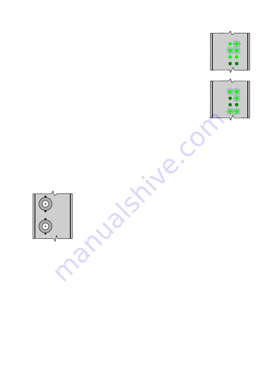
If both the primary and secondary input data rates do not match the set data rate, both the 
primary and secondary INPUT LEDs and their corresponding data rate LEDs will flash. Being 
set up as a single 1 In, 8 Out DA, the both data rate LEDs of the primary input will flash. This 
shows which input has been set up as the primary input. 
 
In this example the primary input is ‘IN A’ and its corresponding data rate is at the 3G rate. 
The secondary input is ‘IN B’ and its corresponding data rate is at the SD rate. The set data 
rate is obviously set for HD-SDI only as neither INPUT A (3G-SDI) nor INPUT B (SD-SDI) take 
control. 


Non-Reclocking Mode:


The rate set only applies to the reclocking mode. In non-reclocking mode the reclocker is bypassed allowing other 
data rates to pass through. Whilst in the non-reclocking mode, if an input signal is present, the corresponding front 
panel INPUT LED will illuminate, but the 3G, HD and SD LEDs will not except in the case where the input data rate 
actually  corresponds  to  a  3G,  HD  or  SD  rate.  Likewise,  in  the  reclocking  mode,  if  an  input  is  not  at  one  of  the 
standard 3G, HD or SD rates the INPUT LED will flash and none of the 3G, HD or SD LEDs will illuminate or flash. 


Front Panel Monitor Outputs:


With  the  DDA-4010  set  up  as  a  Single  1  In,  8  Out  Distribution  Amplifier  with  Automatic 
Changeover  disabled,  the  ‘CH.A’  and  ‘CH.B’  BNC  connectors  on  the  front  panel  both 
monitor the primary input. 
 
With  Automatic  Changeover  enabled,  the  ‘CH.A’  BNC  connector  monitors  the  signal 
connected  to  INPUT A  and  the  ‘CH.B’  BNC  connector  monitors  the  signal  connected  to 
INPUT B. 


Relay Bypass Option:


With the DDA-4010 fitted with the optional ZDA-4010RL relay bypass rear assembly, on loss of power or removal of 
the card from the frame, the INPUT A signal is automatically routed via a relay to the output ‘OUT 1A’ port, as is 
the INPUT B signal to the output ‘OUT 1B’ port. Thus if the DDA-4010 is being run in the single 1 In, 8 Out mode, if 
anything  is  connected  to  the  secondary  input  port,  whether  the  Automatic  Changeover  mode  is  enabled  or  not, 
the secondary input is also routed to one of the outputs. Caution should therefore be observed when connecting 
to the secondary input to connect the correct signal if using the Automatic Changeover mode, or not connecting a 
signal  to  the  secondary  input  at  all  with  the  Automatic  Changeover  disabled,  when  using  the  relay  bypass  rear 
assembly. 
 

A  B 

INPUT 

SD 

HD 

3G 

CH.A 

CH.B 

A  B 

INPUT 

SD 

HD 

3G 

Содержание DDA-4010

Страница 1: ...DDA 4010 IRT Electronics Pty Ltd www irtelectronics com Page 1 of 21 Revision 01 Single 1 In 8 Out Dual 1 In 4 Out 3G HD SD ASI Reclocking Non Reclocking Distribution Amplifier User Manual...

Страница 2: ...By Change Description Applicable to 00 03 01 2013 AL Original Issue Issue 3 PCB units fitted with firmware version 2 1 01 03 06 2013 AL DIP switch designators changed to SW1 and SW2 links LK1 and LK2...

Страница 3: ...arm Outputs 11 Front and Rear Layouts 12 Operation 13 Single 1 In 8 Out Mode 13 ChAx8 Input A to all 8 Outputs 13 ChBx8 Input B to all 8 Outputs 13 Automatic Changeover Mode 13 Non Reclocking Mode 14...

Страница 4: ...itions dangerous potentials may exist in some circuits when power controls are in the OFF position Maintenance personnel should observe all safety regulations Do not make any adjustments inside equipm...

Страница 5: ...present and whether the outputs are locked to the inputs An optional relay bypass rear assembly is available to switch the Inputs to one of their respective Outputs in the event of a power failure Si...

Страница 6: ...HD LED green x2 when HD SDI signal present and locked to selected input on either A or B outputs 3G LED green x2 when 3G SDI signal present and locked to selected input on either A or B outputs Alarm...

Страница 7: ...SW2 2 Auto Detect 3G HD SD ASI rates OFF OFF SD SDI ASI only ON OFF HD SDI only OFF ON 3G SDI only ON ON SW2 3 OFF I P B Reclocking mode DA behaves as a Reclocking DA ON I P B Non Reclocking mode Recl...

Страница 8: ...puts if desired ChBx8 Input B to all 8 Outputs 4 x Output A and 4 x Output B Sw1 5 OFF Single 1 In 8 Out DA mode Sw2 5 ON Input B primary input Data Rate For automatic detection of signal type so that...

Страница 9: ...ing Mode Sw1 3 OFF Input A reclocked A input behaves as a reclocking DA Sw2 3 OFF Input B reclocked B input behaves as a reclocking DA Non Reclocking Mode Sw1 3 ON Input A non reclocked A input behave...

Страница 10: ...nputs Outputs For use with supplied standard rear assembly ZDA 4010 or optional relay bypass rear assembly ZDA 4010RL The DDA 4010 can be configured as a single 1 IN 8 OUT distribution amplifier or as...

Страница 11: ...hBx8 mode alarm A is non functional regardless of input A s status unless automatic changeover mode is also set If in the dual ChAx4 ChBx4 mode both alarms A and B are functional regardless of whether...

Страница 12: ...DDA 4010 IRT Electronics Pty Ltd www irtelectronics com Page 12 of 21 Revision 01 Front rear panel connector diagrams ZDA 4010 Standard Rear Assembly ZDA 4010RL 3G HD SD ASI Relay Bypass Rear Assembly...

Страница 13: ...t data rate signal such as HD SDI Unless Automatic Changeover mode has been implemented even if a signal has been applied to the IN A port INPUT A will not illuminate See Automatic Changeover descript...

Страница 14: ...ode if an input signal is present the corresponding front panel INPUT LED will illuminate but the 3G HD and SD LEDs will not except in the case where the input data rate actually corresponds to a 3G H...

Страница 15: ...data rate the corresponding input and detected data rate LEDs will flash and the corresponding outputs will be muted unless the Automatic Changeover function has been implemented see Automatic Change...

Страница 16: ...nd B has been set for the SD SDI only rate Input A is being fed by a signal at the SD rate which is being fed to B s outputs as indicated by the INPUT A LED not flashing whilst A s SD data rate LED is...

Страница 17: ...ion and translates that information into a form compatible with SNMP The agent therefore acts as an interface between the NMS and the managed devices The NMS sends a request message and control comman...

Страница 18: ...that are SNMP compatible may need an optional plug in SNMP module with a program relevant to the module that it is plugged into Depending on the module besides the module identification parameters su...

Страница 19: ...x4 Dual 1x4 DA IN A OUT 1A to OUT 4A IN B OUT 1B to OUT 4B 2 chAx8 Single1x8DA INAprimaryinput INA OUT1AtoOUT4A OUT1BtoOUT4B 3 chBx8 Single1x8DA INBprimaryinput INB OUT1BtoOUT4B OUT1AtoOUT4A autoChang...

Страница 20: ...Reclocker enable bypass option is not applicable to the secondary input of a single 1x8 DA mode If the user sets this parameter to na the reclocker will default to the enabled setting alias A 16 chara...

Страница 21: ...re Warranty on components shall be extended by IRT only to the extent obtainable from the component supplier Equipment return Before arranging service ensure that the fault is in the unit to be servic...

Отзывы: