background image

2

July 6, 2010

AN1559.0

QHx220 System Overview

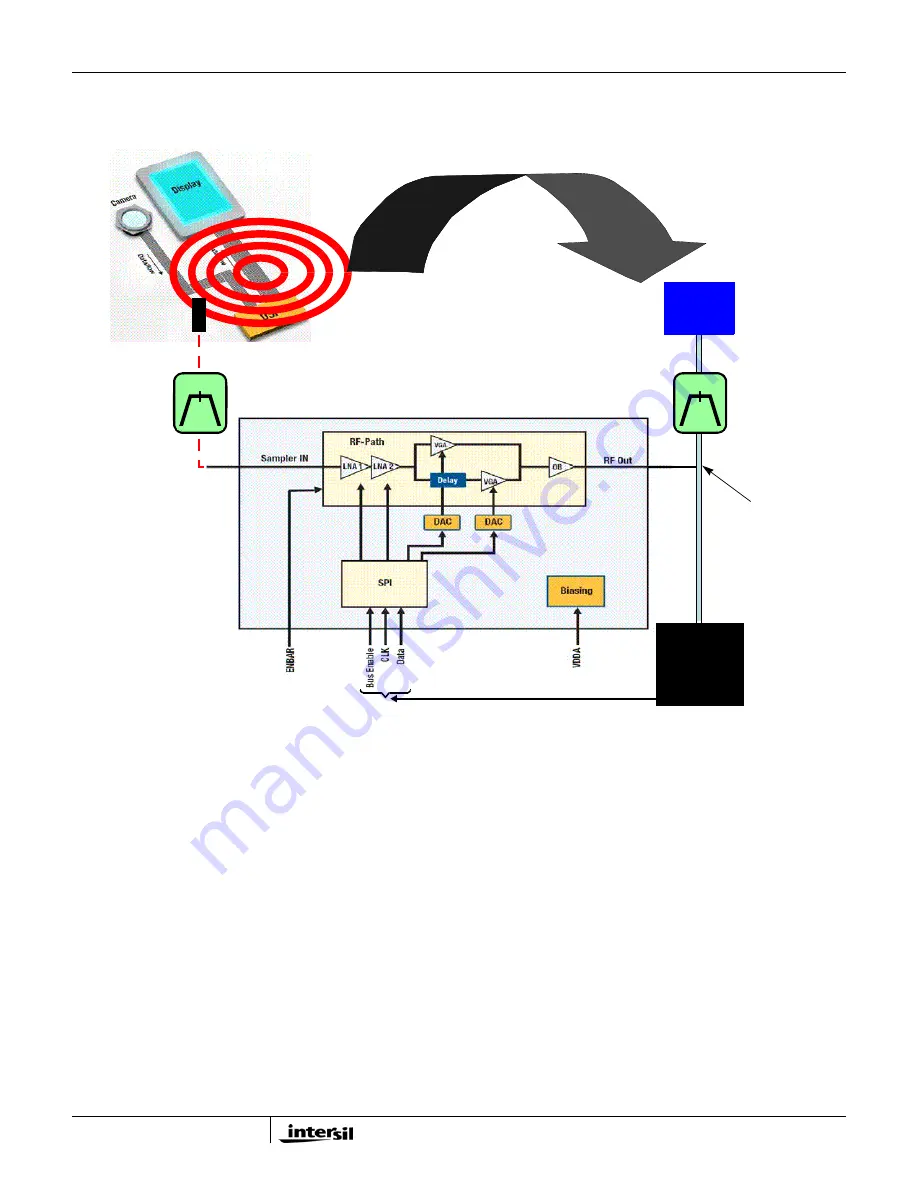
General Application System Block Diagram for QHx220

Description of QHx220 System Block 

Diagram

The block diagram shown in Figure 1 illustrates the 
typical system architecture for the implementation of the 
QHx220 noise canceller. The QHx220 integrates the LNA 
gain stages in the sampler path as well as the DACs 
which control the I and Q (or ultimately the gain and 
phase) of the device. The LNA gain stages and the I and 
Q are controlled via the SPI bus interface. The GUI 
software supplied with the evaluation board provides a 
means to manually tune all of these parameters. 

A known noise source is sampled by a variety of tapping 
methods depending on the accessibility of sampling the 
noise source. The sampled noise is then filtered by a 
bandpass filter that has the same bandwidth as the 
victim receive band. It may be possible to eliminate this 
filter stage. However, this is dependent on the 
characteristics of the aggressor source, the sampling 
methodology and the location of the cancellation node 

within the receiver chain. The QHx220 has internal LNA 
gain stages that can be set to pre-amplify the sampled 
input noise if necessary. The amount of pre-amplification 
required (if any) depends on coupling factors between 
the noise source and the victim antenna as well as the 
level of the sampled noise at the input of the QHx220. 
Since the dynamic range of the QHx220 is typically 50dB, 
the noise level at the input of the QHx220 should be 
approximately 25dB higher than the noise level present 
at the victim receiver (when using the minimum gain 
setting). Higher gain settings should be used when it is 
not possible to find a strong enough tapping point of the 
noise source. Setting this level correctly will allow for a 
maximum tuning range when using the QHx220 tuning 
control. This characterization will determine the amount 
of pre-amplification necessary for any given application. 
It is important to remember not to exceed the -45dBm 
maximum input power of the QHx220 device. The 
QHx220 has a high output impedance which only 
introduces, on the order of tenths of a dB, insertion loss 

FIGURE 1. TYPICAL APPLICATION DIAGRAM

SAMPLER

CANCELLATION 

NODE

COUPLING CHANNEL

VICTIM

ANTENNA


NOISE SOURCE

SIGNAL INTEGRITY

VIA SPI BUS

VICTIM

RECEIVER

AND

BASEBAND

PARAMETER FEEDBACK 


F

C

F

C

QHx220

Application Note 1559

Содержание QHx220

Страница 1: ...10 QHx220 Board Layout 10 QHx220 Board Schematics for GPS 11 QHx220 Board Bill of Materials for GPS 12 GPS Optimization Setup Static Coupling Channel 12 GPS Application Setup 14 WLAN Product Application 15 QHx220 Board Layout 15 QHx220 Board Schematics for WLAN 16 QHx220 Board Bill of Materials for WLAN 17 WLAN Optimization Setup Static Coupling Channel 17 WLAN Application Setup 19 Q ACTIVE 19 CAU...

Страница 2: ...he QHx220 has internal LNA gain stages that can be set to pre amplify the sampled input noise if necessary The amount of pre amplification required if any depends on coupling factors between the noise source and the victim antenna as well as the level of the sampled noise at the input of the QHx220 Since the dynamic range of the QHx220 is typically 50dB the noise level at the input of the QHx220 s...

Страница 3: ...0 device It is often necessary to try multiple tapping points and tapping methods in order to achieve the best possible correlation to the noise present in the victim antenna 3 Be sure to choose the correct level of pre amplification as described in the previous sections If this is not set correctly it will limit the tuning range of the QHx220 device and hence limit the amount of cancellation that...

Страница 4: ...gs into the USB port of the PC and is used to control the SPI bus interface of the QHx220 device The USB controller board also has a 1 8V regulated supply that is used to power the QHx220 device The user may alternatively power the device with an external power supply if so desired A custom cable is also provided which is keyed so that it plugs into the USB controller board in the correct orientat...

Страница 5: ...rview on how the QHx220 can be applied for use in Mobile TV product applications QHx220 Board Layout SPI INTERFACE NOISE SAMPLER INPUT INTERSIL QHx220 1 8V INPUT Rx INPUT FROM ANTENNA Rx OUTPUT TO RECEIVER GND LED FIGURE 5 QHx220 EVALUATION BOARD LAYOUT MTV Application Note 1559 ...

Страница 6: ...6 July 6 2010 AN1559 0 QHx220 Board Schematics for MTV FIGURE 6 SCHEMATIC OF QHx220 EVALUATION BOARD MTV Application Note 1559 ...

Страница 7: ...e coupling loss between the aggressor source and the MTV victim antenna For the purpose of this evaluation the attenuator should be roughly 10dB to 20dB for a typical coupling factor Keep in mind that the second power splitter adds an additional 6dB to the coupling factor Since the QHx220 has 50dB dynamic range this range of attenuation should set the aggressor power in the middle of the tuning ra...

Страница 8: ...sired frequency Figure 8 is an example of the type of cancellation that should be achieved when the I and Q values have been optimized Once the cancellation has been optimized record the I and Q values for the optimization of the setup used FIGURE 7 MTV OPTIMIZATION SETUP DIAGRAM ATTENUATOR PAD TO SET COUPLING LOSS MTV AGGRESSOR NETWORK ANALYZER QHx220 CANCELLATION NODE POWER SPLITTER PORT 1 PORT ...

Страница 9: ...that degrades the receive signal strength reported by the MTV receiver turn on the QHx220 board and set the optimized I and Q values that were determined in the MTV Optimization Setup Static Coupling Channel section on page 7 This should result in a 15dB recovery of the receive signal strength power reported by the MTV receiver if the board was optimized correctly However since the setup was sligh...

Страница 10: ...overview on how the QHx220 can be applied for use in GPS product applications QHx220 Board Layout SPI INTERFACE INTERSIL QHx220 1 8V INPUT Rx INPUT FROM ANTENNA Rx OUTPUT TO RECEIVER GND LED NOISE SAMPLER INPUT FIGURE 10 QHx220 EVALUATION BOARD LAYOUT GPS Application Note 1559 ...

Страница 11: ...ND1 C4 10nF GND1 1V8 L2 100nH C5 100pF D1 LED R2 220 1V8 GND1 GND2 GND1 C6 C_Select L3 L_Select GND1 L4 L_Option C7 C_Option GND1 1V8 R0 DNI 1 2 JP 1 1 2 3 4 JP 2 SPI L7 10k L6 14k L5 10k R5 14k R4 14k R3 14k GND1 GND1 GND1 QHx220 GND1 1 GND1 3 IN 2 ENBAR 4 VDDD 5 CLK 6 DATA 7 EXTR 8 BUS 9 GND2 10 RF 11 GND2 12 VDDA 13 VDDA 14 IND 15 GND2 16 U1 FIGURE 11 SCHEMATIC OF QHx220 EVALUATION BOARD GPS Ap...

Страница 12: ...nts the coupling loss between the aggressor source and the GPS victim antenna For the purpose of this evaluation the attenuator should be roughly 10dB to 20dB for a typical coupling factor Keep in mind that the second power splitter adds an additional 6dB to the coupling factor Since the QHx220 has 50dB dynamic range this range of attenuation should set the aggressor power in the middle of the tun...

Страница 13: ...le of the type of cancellation that should be achieved when the I and Q values have been optimized Once the cancellation has been optimized record the I and Q values for the optimization of the setup used ATTENUATOR PAD TO SET COUPLING LOSS GPS AGGRESSOR NETWORK ANALYZER QHX220 CANCELLATION NODE POWER SPLITTER PORT 1 PORT 2 POWER SPLITTER 50Ω TERMINATION PATH FIGURE 12 GPS OPTIMIZATION SETUP DIAGR...

Страница 14: ...es the receive signal strength reported by the GPS receiver turn on the QHx220 board and set the optimized I and Q values that were determined in the GPS Optimization Setup Static Coupling Channel section on page 12 This should result in a 15dB recovery of the receive signal strength power reported by the GPS receiver if the board was optimized correctly However since the setup was slightly modifi...

Страница 15: ...verview on how the QHx220 can be applied for use in WLAN product applications QHx220 Board Layout SPI INTERFACE INTERSIL QHX220 1 8V INPUT Rx INPUT FROM ANTENNA Rx OUTPUT TO RECEIVER GND LED NOISE SAMPLER INPUT FIGURE 15 QHx220 EVALUATION BOARD LAYOUT WLAN Application Note 1559 ...

Страница 16: ...ND1 C4 10nF GND1 1V8 L2 100nH C5 100pF D1 LED R2 220 1V8 GND1 GND2 GND1 C6 C_Select L3 L_Select GND1 L4 L_Option C7 C_Option GND1 1V8 R0 DNI 1 2 JP1 1 2 3 4 JP 2 SPI L7 10k L6 14k L5 10k R5 14k R4 14k R3 14k GND1 GND1 GND1 QHX2 20 GND1 1 GND1 3 IN 2 ENBAR 4 VDDD 5 CLK 6 DATA 7 EXTR 8 BUS 9 GND2 10 RF 11 GND2 12 VDDA 13 VDDA 14 IND 15 GND2 16 U1 FIGURE 16 SCHEMATIC OF QHx220 EVALUATION BOARD WLAN A...

Страница 17: ...resents the coupling loss between the aggressor source and the WLAN victim antenna For the purpose of this evaluation the attenuator should be roughly 10dB to 20dB for a typical coupling factor Keep in mind that the second power splitter adds an additional 6dB to the coupling factor Since the QHx220 has 50dB dynamic range this range of attenuation should set the aggressor power in the middle of th...

Страница 18: ...ntil the maximum attenuation is achieved at the desired frequency Figure 18 is an example of the type of cancellation that should be achieved when the I and Q values have been optimized ATTENUATOR PAD TO SET COUPLING LOSS WLAN AGGRESSOR NETWORK ANALYZER QHX220 CANCELLATION NODE POWER SPLITTER PORT 1 PORT 2 POWER SPLITTER 50Ω TERMINATION PATH FIGURE 17 WLAN OPTIMIZATION SETUP DIAGRAM 90 40 30 20 10...

Страница 19: ...ues that were determined in the WLAN Optimization Setup Static Coupling Channel section on page 17 This should result in a 15dB recovery of the receive signal strength power reported by the WLAN receiver if the board was optimized correctly However since the setup was slightly modified from the original optimization setup it should be possible to fine tune the QHx220 to improve the in band noise c...

Страница 20: ...Mouser Electronics Authorized Distributor Click to View Pricing Inventory Delivery Lifecycle Information Intersil EBH220BWIMAX EVALZ ...

Отзывы: