background image

User Guide 113

UG113.0

February 15, 2017

Submit Document Feedback

3

PCB Layout Considerations

The PCB layout is critical for proper operation of the ISL85014. 
The following guidelines should be followed to achieve good 
performance.

1. Use a multilayer PCB structure to achieve optimized 

performance. A four-layer PCB is recommended for this design.

2. Use a combination of bulk capacitors and smaller ceramic 

capacitors with lower ESL for the input capacitors, and place 
them as close to the IC as possible. 

3. Place the VDD decoupling capacitor close to the IC between 

VDD and GND. A 1µF


ceramic capacitor is typically used.

4. Place a bootstrap capacitor close to the IC between the BOOT 

and PHASE pins. A 0.1µF


ceramic capacitor is typically used.

5. Connect the feedback resistor divider between the output 

capacitor positive terminal and AGND pin of the IC, and place 
the resistors close to the FB pin of the IC. 

6. Connect the GND of the IC to the ground planes underneath 

using multiple thermal vias to improve thermal performance.

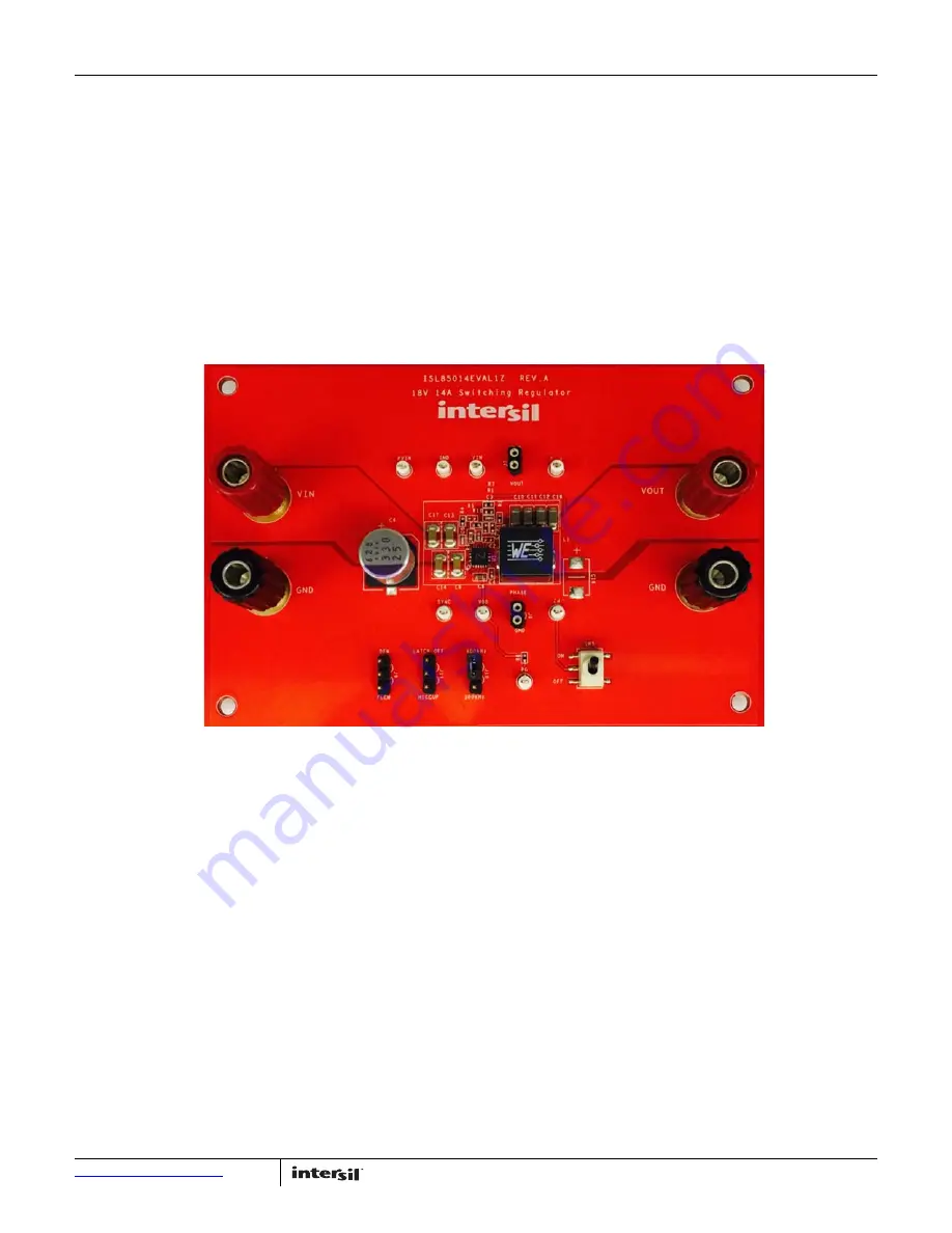
ISL85014EVAL1Z Evaluation Board

FIGURE 2. TOP VIEW

Содержание ISL85014EVAL1Z

Страница 1: ...equency synchronization option Jumper selectable mode DEM Forced CCM Jumper selectable OCP mode Hiccup Latch off Jumper selectable frequency 600kHz 300kHz Connectors and test points for easy probing Compact design Related Literature For a full list of related documents visit our website ISL85014 product pages Ordering Information PART NUMBER DESCRIPTION ISL85014EVAL1Z Evaluation board for ISL85014...

Страница 2: ...he load current to 0 1A and turn on the power supply The output voltage should be in regulation with a nominal 1 8V output 7 Slowly increase the load up to 14A while monitoring the output voltage which should remain in regulation with a nominal 1 8V output 8 Slowly sweep VIN from 4 5V to 18V The output voltage should remain in regulation with a nominal 1 8V output 9 Decrease the input voltage to 0...

Страница 3: ...he input capacitors and place them as close to the IC as possible 3 Place the VDD decoupling capacitor close to the IC between VDD and GND A 1µF ceramic capacitor is typically used 4 Place a bootstrap capacitor close to the IC between the BOOT and PHASE pins A 0 1µF ceramic capacitor is typically used 5 Connect the feedback resistor divider between the output capacitor positive terminal and AGND p...

Страница 4: ...G C11 100uF J2 1 R7 20 J4 1 R5 DNP C7 1nF J11 1 2 3 R9 0 J1 1 C16 DNP J3 1 C9 22uF VOUT SYNC C14 22uF VDD C6 330uF 25V J7 1 2 C8 2 2uF R2 100k PVIN R6 100k C10 100uF SW5 SW SPDT U1 ISL85014 SYNC 1 2 MODE 3 FREQ PG 4 VDD 5 BOOT 6 7 GND 9 PVIN 8 PHASE FB 10 COMP 11 NC 12 NC1 13 EN 14 VIN 15 VIN R1 200k R4 100k R3 DNP C4 100n C13 22uF C1 DNP EN L1 0 68uH C2 DNP GND J9 1 2 3 C5 1u C3 DNP J6 1 2 J10 1 ...

Страница 5: ...HITE ROHS 5002 KEYSTONE J9 J10 J11 3 CONN HEADER 1x3 BREAKAWY 1x36 2 54mm ROHS 68001 203HLF BERG FCI L1 1 COIL PWR CHOKE SMD 10x10x9 0mm 0 68µH 20 ROHS 7443330068 WURTH ELEKTRONIK R7 1 RES SMD 0402 20Ω 1 16W 1 TF ROHS ERJ2RKF20R0 PANASONIC R9 1 RES SMD 0402 0Ω 1 16W 5 TF ROHS CR0402 16W 00T VENKEL R2 R4 R6 3 RES SMD 0402 100k 1 16W 1 TF ROHS ERJ2RKF1003 PANASONIC R10 1 RES SMD 0402 200Ω 1 16W 1 TF...

Страница 6: ...User Guide 113 UG113 0 February 15 2017 Submit Document Feedback 6 ISL85014EVAL1Z PCB Layout FIGURE 4 TOP LAYER FIGURE 5 LAYER 2 FIGURE 6 LAYER 3 FIGURE 7 BOTTOM LAYER ...

Страница 7: ...February 15 2017 Submit Document Feedback Typical Performance Curves VIN 12V VOUT 1 8V L 0 68µH fSW 600kHz TA 25 C unless otherwise noted FIGURE 8 EFFICIENCY vs LOAD FIGURE 9 START UP WITH EN IOUT 14A FIGURE 10 LOAD TRANSIENT 0A 14A 0A 2 5A µs FIGURE 11 OUTPUT VOLTAGE RIPPLE IOUT 14A 30 40 50 60 70 80 90 100 0 2 4 6 8 10 12 14 OUTPUT CURRENT A VIN 12V fsw 600kHz DEM VIN 5V fsw 600kHz DEM EFFICIENC...

Отзывы: