background image

UG105 Rev.0.00

Page 9 of 14

Aug 14, 2017

ISL8215MEVAL1Z

3. PCB Layout Guidelines

3.4

Typical Evaluation Board Performance Data

Operating condition: V

IN

 = 24V, f

SW

 = 300kHz, CCM Mode, unless otherwise noted. 

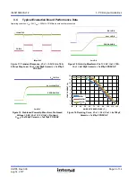
Figure 11. Transient Response, V

OUT

 = 3.3V, 0A to 7.5A, 

2.5A/µs Step Load, C

OUT

 = 4x100µF C 1x470µF 

POSCAP

Figure 12. Start-Up Waveform, V

OUT

 = 3.3V, I

OUT

 = 15A, 

C

OUT

= 4x100µF C 1x470µF POSCAP

Figure 13. Prebiased Power-Up Waveform, Prebiased 

Voltage = 3.0V, V

OUT

 = 3.3V, I

OUT

 = No Load, 

C

OUT

= 4x100µF C 1x470µF POSCAP

Figure 14. Derating Curve, V

OUT

 = 3.3V, C

OUT

 = 4x100µF 

C 1x470µF POSCAP

100mV/DIV

5A/DIV

500µs/DIV

V

OUT

 1V/DIV

PGOOD 2V/DIV

5ms/DIV

EN 1V/DIV

V

OUT

 100mV/DIV

PGOOD 2V/DIV

5ms/DIV

V

IN

 12V/DIV

0

2

4

6

8

10

12

14

16

25

35

45

55

65

75

85

95

105

115

125

AMBIENT TEMPERATURE (°C)

0LFM

200LFM

400LFM

L

O

AD CURRENT (

A)

Содержание ISL8215MEVAL1Z

Страница 1: ...Rev 0 00 Aug 2017 User s Manual ISL8215MEVAL1Z User s Manual Evaluation Board Industrial Analog and Power ...

Страница 2: ...through the SYNC pin A selectable Pulse Skipping Mode PSM with Diode Emulation Mode DEM can be enabled easily to improve light load efficiency for battery related applications The evaluation board also features output voltage tracking which can be implemented through the SS TRK pin By default the board is set to a 3 3V output voltage with a 300kHz switching frequency 1 1 Key Features Wide input vo...

Страница 3: ... supply with at least 12A source current capability Electronic loads capable of sinking current up to 15A Digital Multimeters DMMs Oscilloscope with higher than 100MHz bandwidth Figure 1 ISL8215MEVAL1Z Block Diagram ISL8215M 7V TO 42V INPUT CIN COUT 3 3V 15A OUTPUT 20 100k ENABLE POWER GOOD 10µF 47nF 2 1µF 9 53k DNP 4 02 270pF PH VIN1 VIN VOUT EN PGOOD VCC MOD SYNC RT SS TRK SGND UG1 UG2 COMP VOUT...

Страница 4: ...ltage VIN within the specified range and observe output voltage The output voltage variation should be within 1 5 7 Adjust the load current to within the specified range 0 15A and observe output voltage The output voltage variation should be within 1 5 8 To change VOUT disconnect the evaluation board from the setup and populate a standard 0603 resistor at the R2 placeholder location on the bottom ...

Страница 5: ...VOUT point is connected to the Remote Sense RS pin by routing the trace through inner Layer 3 A 2Ω resistor is placed close to the RS pin for damping the noise on the traces 5 To avoid ground bouncing issues place the VIN return and the VOUT return diagonally opposite to each other This ensures that the switching noise generated by the power train will have a minimal effect on the controller opera...

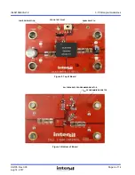
Страница 6: ...age 6 of 14 Aug 14 2017 ISL8215MEVAL1Z 3 PCB Layout Guidelines Figure 2 Top of Board Figure 3 Bottom of Board ENABLE SWITCH PGOOD TEST POINT CCM DEM SELECTION VOUT PROGRAMMING RESISTOR SW FREQUENCY PROGRAMMING RESISTOR ...

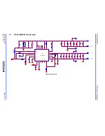
Страница 7: ...C19 TP1 TP5 J3 575 4 R8 40 2K DNP C26 C3 0 047UF 1UF C25 C21 DNP R9 100K 575 4 J4 ISL8215MIRZ U1 PAD1 SGND A2 SS TRK A3 RT A4 PGOOD A5 MOD SYNC E3 VCC A6 EN E2 OCS A8 EN C8 NC1 K4 UG2 D8 NC2 D6 UG1 A1 COMP PAD4 VIN C1 FB B7 VIN1 PAD3 PGND D1 RS E1 VOUT1 PAD2 VOUT PAD5 PHASE 4 02 R1 10UF C22 SW1 GT12MSCBE 1 3 C10 DNP 100UF C27 R10 DNP J1 575 4 100UF C12 10UF C18 DNP C20 C2 270pF R2 9 53K DNP C16 C1...

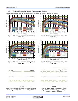
Страница 8: ...out 300kHz 1Vout 300kHz 1 2Vout 300kHz 1 5Vout 300kHz 1 8Vout 300kHz 2 5Vout 300kHz 3 3Vout 300kHz 5Vout 300kHz EFFICIENCY LOAD CURRENT A 60 65 70 75 80 85 90 95 100 0 1 2 3 4 5 6 7 8 9 10 11 12 13 14 15 0 9Vout 300kHz 1Vout 300kHz 1 2Vout 300kHz 1 5Vout 300kHz 1 8Vout 300kHz 2 5Vout 300kHz 3 3Vout 300kHz 5Vout 300kHz 12Vout 600kHz EFFICIENCY LOAD CURRENT A 55 60 65 70 75 80 85 90 95 100 0 1 2 3 4...

Страница 9: ...gure 12 Start Up Waveform VOUT 3 3V IOUT 15A COUT 4x100µF Ceramic 1x470µF POSCAP Figure 13 Prebiased Power Up Waveform Prebiased Voltage 3 0V VOUT 3 3V IOUT No Load COUT 4x100µF Ceramic 1x470µF POSCAP Figure 14 Derating Curve VOUT 3 3V COUT 4x100µF Ceramic 1x470µF POSCAP 100mV DIV 5A DIV 500µs DIV VOUT 1V DIV PGOOD 2V DIV 5ms DIV EN 1V DIV VOUT 100mV DIV PGOOD 2V DIV 5ms DIV VIN 12V DIV 0 2 4 6 8 ...

Страница 10: ...met C0402C473J3RAC7867 Multilayer Capacitor C25 1 1 0µF 10 25V 0603 Murata GRM188R71E105KA12D Ceramic Chip Capacitor C7 1 OPEN 10 25V 0402 Generic Multilayer Capacitor C1 1 0 1µF 10 25V 0603 Murata GRM188R71E104KA01D Ceramic Capacitor C2 Note 1 1 270pF 10 100V 0603 Murata GRM188R72A271KA01D Ceramic Capacitor C24 1 10µF 10 25V 0805 TDK C2012X5R1E106K Multilayer Capacitor J1 J4 4 CONN JACK Keystone ...

Страница 11: ...or R9 1 100kΩ 1 1 10W 0603 Venkel CR0603 10W 1003FT Chip Resistor R7 1 26 1kΩ 1 1 10W 0603 Yageo 9C06031A2612FKHFT Chip Resistor R8 1 40 2kΩ 1 1 10W 0603 Yageo RC0603FR 0740K2L Chip Resistor R16 1 2Ω 1 1 16W 0402 Venkel CR0402 16W 02R0FT Chip Resistor Note 1 R1 and C2 do not have a reference designator or footprint on the evaluation board The resistor and capacitor are soldered on the bottom of th...

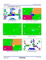
Страница 12: ...7 ISL8215MEVAL1Z 3 PCB Layout Guidelines 3 6 ISL8215MEVAL1Z PCB Layout Figure 15 Silkscreen Top Figure 16 Top Layer Component Side Figure 17 Inner Layer 2 Figure 18 Inner Layer 3 Figure 19 Bottom Layer Solder Side Figure 20 Silkscreen Bottom ...

Страница 13: ...ed to verify that the document is current before proceeding For information regarding Intersil Corporation and its products see www intersil com Copyright Intersil Americas LLC 2017 All Rights Reserved All trademarks and registered trademarks are the property of their respective owners UG105 Rev 0 00 Page 13 of 14 Aug 14 2017 4 Revision History Rev Date Description 0 00 Aug 14 2017 Initial release...

Страница 14: ...ISL8215MEVAL1Z UG105 ...

Отзывы: