background image

AP440FX Motherboard Technical Product Specification

46

The disk-based Flash upgrade utility, FMUP.EXE, has three options for BIOS upgrades:

• 

The Flash BIOS can be updated from a file on a disk.

• 

The current BIOS code can be copied from the Flash EEPROM to a disk file as a backup in the
event that an upgrade cannot be successfully completed.

• 

The BIOS in the Flash device can be compared with a file to ensure the computer has the
correct version.

The upgrade utility ensures the upgrade BIOS extension matches the target computer to prevent
accidentally installing a BIOS for a different type of computer.

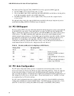
3.4  PCI IDE Support

The two local bus IDE connectors with independent I/O channel support are setup up automatically
by the BIOS if the user selects “Autoconfiguration” in Setup.  The IDE interface supports PIO
Mode 3, and Mode 4 hard drives and recognition of ATAPI CD-ROMs, tape drives, and any other
ATAPI devices.  The BIOS determines the capabilities of each drive and configures them to
optimize capacity and performance.  For the high capacity hard drives typically available, the drive
is automatically configured for Logical Block Addressing (LBA) for maximum capacity and to
PIO Mode 3 or 4 depending on the capability of the drive.  The user can override the auto-
configuration options by using the manual mode setting.  The ATAPI Specification Revision 2.5
recommends that an ATAPI device be configured as shown in Table 34.

Table 34.

Recommendations for Configuring an ATAPI Device

Primary Cable

Secondary Cable

Drive 0

Drive 1

Drive 0

Drive 1

ATA

Normal, no ATAPI

ATA

ATAPI

Disk and CD-ROM for enhanced
IDE systems

ATA

ATAPI

Legacy IDE System with only one
cable

ATA

ATAPI

ATAPI

Enhanced IDE with CD-ROM and
a tape or two CD-ROMs

3.5 PCI Auto-Configuration

The PCI auto-configuration utility operates in conjunction with the Setup utility to allow the
insertion and removal of PCI cards without user intervention (Plug and Play).  When the computer
is turned on after adding a PCI add-in card, the BIOS automatically configures interrupts, I/O
space, and other parameters.  PCI interrupts are distributed to available ISA interrupts that have not
been assigned to an ISA card, or other resources.  Those interrupts left set to “available” in Setup
are considered free for PCI add-in card use.

The PCI Auto-Configuration function complies with version 2.10 of the PCI BIOS specification.
Configuration information is stored in ESCD format.  The ESCD data may be cleared (i.e., “write
protection” is removed) by setting the CMOS clear jumper to the DOWN (CLR) position.

Содержание AP440FX

Страница 1: ...0FX motherboard may contain design defects or errors known as errata which may cause the product to deviate from published specifications Current characterized errata are documented in the AP440FX Motherboard Specification Update May 1997 Order Number 281830 002 ...

Страница 2: ...s for a particular purpose merchantability or infringement of any patent copyright or other intellectual property right Intel products are not intended for use in medical life saving or life sustaining applications Intel retains the right to make changes to specifications and product descriptions at any time without notice The AP440FX motherboard may contain design defects or errors known as errat...

Страница 3: ... 15 1 8 2 Keyboard and Mouse Interface 15 1 8 3 Real Time Clock CMOS RAM and Battery 16 1 8 4 Infrared Support 16 1 8 5 Parallel Port 16 1 9 Graphics Subsystem 16 1 9 1 S3 ViRGE Graphics Subsystem 17 1 9 2 S3 ViRGE DX Graphics Subsystem 18 1 9 3 LBP VESA Feature Connector 18 1 9 4 Graphics Drivers and Utilities 18 1 10 Audio Subsystem 19 1 11 Management Extension Hardware 19 1 12 Motherboard Conne...

Страница 4: ...ay 47 3 7 Desktop Management Interface DMI 47 3 8 Advanced Power Management APM 48 3 9 Advanced Power Control APC 48 3 10 Language Support 49 3 11 Boot Options 49 3 12 Flash LOGO Area 49 3 13 Setup Enable Jumper 49 3 14 Overview of the Setup Menu Screens 49 3 14 1 Main BIOS Setup Screen 50 3 14 2 Floppy Options Subscreen 51 3 14 3 IDE Device Configuration Subscreen 52 3 14 4 Boot Options Subscreen...

Страница 5: ...SA Riser Connector J6J2 25 8 LBP VESA Feature Connector J1K1 27 9 Serial Port COM2H J3N1 Pinout 27 10 CD ROM Connector J9N1 28 11 Wavetable Upgrade Connector J9L1 28 12 Telephony Connector J9K1 28 13 Primary Power Supply Connector J9H1 29 14 External 3 3 V Power Supply Connector J9J1 29 15 Soft Off Power Supply Connector J9F1 30 16 Floppy Drive Connector J8L1 30 17 IDE Connectors J8H1 J9H2 31 18 V...

Страница 6: ...of the Setup Menu Screens 50 36 Serial Port Configuration Options 58 37 Parallel Port Configuration Options 59 38 ECP Compatible Configuration Options 60 39 Event Log Subscreens 67 40 Administrative and User Password Functions 68 41 BIOS Beep Codes 71 42 PCI Configuration Error Messages 71 43 Chained PCI Error Messages 72 44 BIOS Error Messages 73 45 ISA NMI Messages 74 ...

Страница 7: ... and software Secure Flash features to protect flash contents from corruption Uses a BIOS that complies with the Desktop Management Interface DMI compliant Uses the National Semiconductor Super I O controller the PC87307 or the pin compatible PC87308 device to integrate the following standard PC I O functions floppy interface two FIFO serial ports and one EPP ECP capable parallel port real time cl...

Страница 8: ...ctor J8L1 N Telephony modem header 2x2 J9K1 O Standard 3 3V power connector J9J1 P Main power connector J9H1 Q IDE connectors J8H1 J9H2 R Soft Off header 3x1 J9F1 S Hardware monitor ASIC U9C1 T Flash BIOS E28F002 U8C1 U Real time clock battery BT9B1 V Onboard speaker L9A1 W 3 5 V processor jumper J8A2 X SIMM sockets J6J1 J7J1 J7J2 J7J3 Y Intel SB82371SB PIIX3 U6E1 Z Auxiliary fan header 1x3 J4A1 A...

Страница 9: ...r The motherboard is designed to fit into a standard LPX form factor chassis Figure 2 illustrates the mechanical form factor for the AP440FX The AP440FX LPX form factor adheres to the standard LPX guidelines with outer dimensions of 9 inches x 13 inches OM06179 5 50 10 98 8 45 12 63 0 150 8 65 0 35 3 55 0 00 7 15 0 00 0 37 7 10 Figure 2 Motherboard Dimensions ...

Страница 10: ...mputers based on the AP440FX motherboard need the back panel I O shield in order to pass certification testing Figure 3 shows the critical dimensions for the I O shield and indicates the position of each cutout 0 682 0 525 0 900 0 235 0 118 2 534 3 945 4 645 6 904 8 193 9 000 0 021 0 080 0 079 0 027 0 075 Right end View OM06183A 5 302 5 963 Figure 3 Back Panel I O Shield Dimensions ...

Страница 11: ...EE standard 754 1985 NOTE If you are installing a 3 5 V processor a jumper must be installed on the jumper block located at J8A2 See Section 1 13 for more information NOTE The 200 MHz Pentium Pro processor with 512 KB of cache memory is not supported on the AP440FX motherboard 1 5 1 Microprocessor Upgrade Socket 8 is a 387 pin modified staggered pin grid array SPGA zero insertion force ZIF socket ...

Страница 12: ...n adding DRAM 1 6 1 DRAM EDO or Hyper Page DRAM is designed to improve the DRAM read performance EDO DRAM holds the memory data valid until the next memory access cycle unlike standard fast page mode DRAM that tri states the memory data when the precharge cycle occurs prior to the next memory access cycle 1 6 2 Parity and ECC DRAM Memory error checking and correction is supported by parity SIMMs W...

Страница 13: ...lerator PIIX3 The 82371SB provides the interface between the PCI and ISA buses and integrates a dual channel fast IDE interface capable of supporting up to four devices The 82371SB integrates four 8 bit and three 16 bit DMA channels three 8 bit timer counters two eight channel interrupt controllers PCI to AT interrupt mapping circuitry NMI logic ISA refresh address generation and PCI ISA bus arbit...

Страница 14: ...oard uses both onboard hardware and BIOS code support to protect the onboard flash memory device from accidentally or intentionally being corrupted A general purpose I O GPIO port of the I O controller is used to control the write enable line of the flash device By putting the microprocessor in System Management Mode SMM whenever the flash write is enabled the BIOS can ensure that the SMM code is ...

Страница 15: ...MB or 2 88 MB 3 media 1 8 1 Floppy Controller The PC87307 is software compatible with the DP8473 and 82077 floppy disk controllers The floppy interface can be configured for 360 KB or 1 2 MB 5 media or for 720 KB 1 2 MB 1 44 MB or 2 88 MB 3 media in the BIOS setup By default the Floppy A interface is configured for 1 44 MB and Floppy B is disabled Configuring the floppy interface for 1 2 MB 3 3 mo...

Страница 16: ...by a trickle current from the power supply 1 8 4 Infrared Support A 5 pin interface on the front panel I O connector allows connection to a Hewlett Packard HSDL 1000 compatible infrared IrDA transmitter receiver Once the module is connected to the front panel I O header Serial port 2 can be redirected to the IrDA module When configured for IrDA the user can transfer files to or from portable devic...

Страница 17: ...dvanced texture mapping features include perspective correction bi linear and tri linear filtering MIP mapping and Z buffering These features provide the most realistic user experience for interactive 3D applications In addition a fast linear addressing scheme based upon DCI reduces software overhead by mapping the display memory into the microprocessor s upper memory address space and permitting ...

Страница 18: ... supported not supported not supported 1600 x 1200 not supported 48 5 IL not supported not supported not supported Non accelerated mode only IL Interlaced The S3 ViRGE DX graphics controller supports more modes than shown above The graphics drivers provide options for additional resolutions 1 9 3 LBP VESA Feature Connector The AP440FX motherboard supports a 34 pin VESA feature connector which also...

Страница 19: ... System MPU 401 CD ROM CS4236 device Each logical device is configured into the host environment using the ISA Plug and Play configuration methodologies The audio subsystem requires up to two DMA channels and one interrupt The computer can be configured to use either DMA channels 0 1 or 3 The interrupt can be mapped to use interrupt 5 7 9 11 12 or 15 1 11 Management Extension Hardware The Manageme...

Страница 20: ...es the I O addresses identified in the I O map 1 12 Motherboard Connectors The AP440FX motherboard has onboard connectors supporting the following feature areas Front panel features Memory SIMM and expansion PCI ISA riser sockets Video features Serial header Audio features Power connectors Floppy and PCI IDE connectors Figure 4 identifies the connectors on the AP440FX motherboard and indicates the...

Страница 21: ...H1 Primary Power 12 Video 34 2 33 1 LPB VESA J1K1 28 Floppy IDE Primary Secondary Front Panel 1 27 J2A1 Front Panel I O Connector Header 1 J3A1 Keylock 1 J9F1 Soft Off 3 1 2 J9L1 Wavetable 7 8 1 33 2 34 5 J8L1 Floppy Drive 40 2 39 1 PCI IDE J8H1 J9H2 J9K1 Telephony 1 1 2 J3N1 COM2H 9 8 Serial 1 J4A1 Aux Fan 3 Figure 4 Motherboard Connector Locations ...

Страница 22: ... Each of the front panel connectors is identified in Figure 4 The front panel I O connector and keyboard lock connector are shown in detail in Figure 5 OM04953 1 27 SPKR SLP IRDA SW_ON PWRLED RESET HDLED 6 13 18 3 J2A1 1 J3A1 Keyboard Lock Figure 5 Front Panel I O Connectors Table 4 lists the pinout for the front panel I O connector Table 4 Front Panel I O Connector J2A1 Pin Signal Name Pin Signal...

Страница 23: ...time out of the inactivity timer Both the keyboard hot key and the inactivity timer are programmable in the BIOS Setup timer is set to 10 minutes by default To reactivate the computer or Resume the user must simply press the sleep resume button again or use the keyboard or PS 2 mouse Mouse activity only wakes up the computer if a mouse driver is loaded While the computer is in Standby or sleep mod...

Страница 24: ...er from these pins 1 12 1 8 Keylock Connector J3A1 The Keylock connector pinout is listed in Table 5 Table 5 Keylock Connector J3A1 Pin Signal Name 1 Ground 2 KB_LOCK 3 Ground 1 12 1 9 Fan Connector J4A1 The auxiliary fan connector J4A1 is a 1 by 3 header that can accept either two position power and ground or three position power ground and fan sense fan plugs Figure 6 indicates the required orie...

Страница 25: ...age 35 for jumper block details Table 7 shows the pinout listing for the PCI ISA riser connector Table 7 PCI ISA Riser Connector J6J2 Pin Signal Name Pin Signal Name Pin Signal Pin Signal Name A1 IOCHK B1 GND E1 GND F1 GND A2 SD7 B2 RSTDRV E2 GND F2 GND A3 SD6 B3 Vcc E3 PCIINT1 F3 PCIINT3 A4 SD5 B4 IRQ9 E4 PCIIINT2 F4 PCIINT4 A5 SD4 B5 5 V E5 Vcc F5 Vcc A6 SD3 B6 DRQ2 E6 Key F6 Key A7 SD2 B7 12 V ...

Страница 26: ...SEL A30 SA1 B30 OSC E30 TRDY F30 PLOCK A31 SA0 B31 GND E31 STOP F31 PERR C1 SBHE D1 MEMCS16 G1 SDONE H1 SERR C2 LA23 D2 IOCS16 G2 SBO H2 AD15 C3 LA22 D3 IRQ10 G3 CBE1 H3 AD14 C4 LA21 D4 IRQ11 G4 PAR H4 AD12 C5 LA20 D5 IRQ12 G5 GND H5 GND C6 LA19 D6 IRQ15 G6 Key H6 Key C7 LA18 D7 IRQ14 G7 GND H7 GND C8 LA17 D8 DACK0 G8 AD13 H8 AD10 C9 MEMR D9 DRQ0 G9 AD11 H9 AD8 C10 MEMW D10 DACK5 G10 AD9 H10 AD7 C...

Страница 27: ...ixel Data 7 17 Ground 18 PCLK Pixel Clock 19 Ground 20 BLANKING 21 Ground 22 HSYNC Horizontal Sync 23 N C not used 24 VSYNC Vertical Sync 25 Key no pin 26 Ground 27 Key no pin 28 Key no pin 29 IICCLK 30 Ground 31 IICDAT 32 N C 33 EN1 34 EN2 1 12 4 Serial Header The COM2 serial port can be accessed using the COM2H header J3N1 on the motherboard Table 9 lists the signals and pinout for the COM2H hea...

Страница 28: ...ovided in Table 10 Table 11 and Table 12 Table 10 CD ROM Connector J9N1 Pin Signal Name 1 Ground 2 CD Left 3 Ground 4 CD Right Table 11 Wavetable Upgrade Connector J9L1 Pin Signal Name 1 Wave Right 2 Ground 3 Wave Left 4 Ground 5 Key 6 Midi_In 7 NC 8 MIDI_Out Table 12 Telephony Connector J9K1 Pin Signal Name 1 Ground 2 Mono Out 3 Mic In 4 Key ...

Страница 29: ...s the ability to determine the state of the power supply so if the computer was turned on when power was disconnected the computer turns back on when power is reapplied or it remains off depending on the user setup configuration in CMOS Table 13 provides the pinout listing for the primary power supply connector of the AP440FX motherboard Table 13 Primary Power Supply Connector J9H1 Pin Name Functi...

Страница 30: ...ndby 2 PS_ON Remote On Off 3 PS_COM Supply presence 1 12 7 Floppy IDE Connectors Table 16 lists the pinout and signal names for the floppy drive connector Table 16 Floppy Drive Connector J8L1 Pin Signal Name Pin Signal Name 1 Ground 2 DENSEL 3 Ground 4 Reserved 5 Key 6 FDEDIN 7 Ground 8 Index 9 Ground 10 Motor Enable A 11 Ground 12 Drive Select B 13 Ground 14 Drive Select A 15 Ground 16 Motor Enab...

Страница 31: ...Data 5 8 Host Data 10 9 Host Data 4 10 Host Data 11 11 Host Data 3 12 Host Data 12 13 Host Data 2 14 Host Data 13 15 Host Data 1 16 Host Data 14 17 Host Data 0 18 Host Data 15 19 Ground 20 Key 21 DDRQ0 DDRQ1 22 Ground 23 I O Write 24 Ground 25 I O Read 26 Ground 27 IOCHRDY 28 Vcc pull down 29 DDACK0 DDACK1 30 Ground 31 IRQ14 IRQ15 32 Reserved 33 DAG1 34 Reserved 35 DAG0 36 DAG2 37 Chip Select 1P 1...

Страница 32: ...A Video Connector Table 18 lists the pinout and signal names for the VGA video connector Table 18 VGA Video Connector J1N1 Pin Signal Name Function Pin Signal Name Function 1 Red Video 9 Key no pin 2 Green Video 10 Sync Return Ground 3 Blue Video 11 Monitor ID Bit 0 not used 4 Monitor ID Bit 2 not used 12 Monitor ID Bit 1 not used 5 Chassis Ground 13 Horizontal Sync 6 Red Return Ground 14 Vertical...

Страница 33: ... Connectors Table 20 lists the pinout and signal names for the USB back panel connectors Table 20 USB Connector Pinout Pin Signal Name 1 5 v fused 2 USBP0 USBP1 fused 3 USBP0 USBP1 fused 4 Ground 1 12 8 4 Keyboard and Mouse Ports Table 21 lists the pinout and signal names for the PS 2 keyboard and mouse connectors Although they are labeled as Keyboard and Mouse on the motherboard and the back pane...

Страница 34: ...FD Auto Feed 2 PPD0 Data Bit 0 15 ERROR Fault 3 PPD1 Data Bit 1 16 INIT Initializing printer 4 PPD2 Data Bit 2 17 SLCTIN Select input 5 PPD3 Data Bit 3 18 GND Chassis Ground 6 PPD4 Data Bit 4 19 GND Chassis Ground 7 PPD5 Data Bit 5 20 GND Chassis Ground 8 PPD6 Data Bit 6 21 GND Chassis Ground 9 PPD7 Data Bit 7 22 GND Chassis Ground 10 ACK Acknowledge 23 GND Chassis Ground 11 BUSY Port Busy 24 GND ...

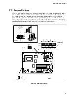
Страница 35: ...rboard configuration parameters The jumper block at J8A2 is used to provide 3 5 V for processors that require that voltage Figure 8 shows the jumper block locations on the motherboard and indicates how jumper placement corresponds to the value defined by the motherboard silk screening Jumper Placement Detail UP DOWN 1 4 3 6 A B 2 5 J4L2 Configuration Jumpers H F D B G E C A UP DOWN PCI Riser J1J1 ...

Страница 36: ...60 30 7 5 DOWN DOWN UP 2 5 166 66 33 8 33 DOWN UP DOWN reserved DOWN UP UP reserved UP DOWN DOWN reserved UP DOWN UP reserved UP UP DOWN 3 180 60 30 7 5 UP UP UP 3 200 66 33 8 33 1 13 2 Motherboard Configuration J4L2 J1J1 The jumpers for sections D E F G and H of J4L2 allow the selection of various motherboard features A second jumper block J1J1 allows selection of a riser board with either two or...

Страница 37: ...le J4L2 G 2 3 J4L2 G 1 2 UP DIS Disable DOWN ENA Enable system password capability SETUP Setup Enable Disable J4L2 H 5 6 J4L2 H 4 5 UP ENA Enable DOWN DIS Disable setup accessibility Riser with 2 PCI slots J1J1 1 2 and J1J1 4 5 Enables use of riser card with two 2 PCI slots Riser with 3 PCI slots J1J1 2 3 and J1J1 5 6 Enables use of riser card with three 3 PCI slots 3 5 V Processor Voltage Jumper ...

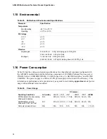
Страница 38: ...hetical computer configured with the AP440FX motherboard and the following components a 200 MHz Pentium Pro processor w 256 KB Cache 16 MB EDO DRAM 3 5 inch floppy drive 1 6 GB IDE hard drive and 4X IDE CD ROM The power supply is a 200 watt LPX power supply with at least 65 efficiency This information is preliminary and is provided only as a guide for calculating approximate total power usage with...

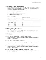
Страница 39: ... 8 0 1 17 Regulatory Compliance This printed circuit assembly complies with the following safety and EMI regulations when correctly installed in a compatible host system 1 17 1 Safety 1 17 1 1 UL 1950 CSA 950 95 3rd edition Dated 07 28 95 The Standard for Safety of Information Technology Equipment including Electrical Business Equipment USA Canada 1 17 1 2 CSA C22 2 No 950 93 3rd Edition The Stand...

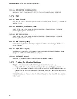
Страница 40: ...ric Immunity Standard Currently compliance is determined via testing to IEC 801 2 3 and 4 Europe 1 17 2 5 VCCI Class 2 ITE Implementation Regulations for Voluntary Control of Radio Interference by Data Processing Equipment and Electronic Office Machines Japan 1 17 2 6 ICES 003 Issue 2 Interference Causing Equipment Standard Digital Apparatus Canada 1 17 3 Product Certification Markings This printe...

Страница 41: ...43K EA000 EBFFF 8K ESCD Plug and Play configuration area 932K 935K E9000 E9FFF 4K Reserved for BIOS 928K 931K E8000 E8FFF 4K OEM LOGO Area 896K 927K E0000 E7FFF 32K BIOS Reserved 800 895K C8000 DFFFF 96K Available HI DOS memory open to ISA and PCI bus 640K 799K A0000 C7FFF 160K Video memory and BIOS 639K 9FC00 9FFFF 1K Extended BIOS Data moveable by QEMM 386MAX 512K 638K 80000 9FBFF 127K Extended ...

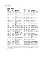
Страница 42: ...bytes PIIX3 DMA Page Register 03F7 bits 6 0 7 bits Pri IDE Chan Status Port 00A0 00A1 2 bytes PIIX3 Interrupt Controller 2 03F8 03FF 8 bytes Onboard Serial Port 1 00C0 00DE 31 bytes PIIX3 DMA 2 04D0 04D1 2 bytes Edge level triggered 00F0 00FF 16 bytes Math Coprocessor Compatible I O Registers LPT 400h 8 bytes ECP port LPT 400h 0170 0177 8 bytes Secondary IDE Channel 0608 060B 4 bytes CS4236 Audio ...

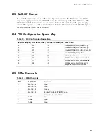
Страница 43: ...ap Table 30 PCI Configuration Space Map Bus Number hex Dev Number hex Function Number hex Description 00 00 00 Intel 82440FX PMC Host Bridge 00 07 00 Intel 82371SB PIIX3 ISA bridge 00 07 01 Intel 82371SB PIIX3 IDE Controller 00 07 02 Intel 82371SB PIIX3 USB 00 08 00 Video Controller 00 13 00 PCI Expansion Slot user available 00 11 00 PCI Expansion Slot user available 00 0B 00 PCI Expansion Slot Op...

Страница 44: ...yboard buffer full 2 Reserved Cascade interrupt from slave PIC 3 Serial Port 2 4 Serial Port 1 5 Audio Codec 6 Floppy 7 Parallel Port 1 8 Real Time Clock 9 Audio FM Synthesis 10 USB 11 Video 12 Onboard Mouse Port if present else user available 13 Reserved Math coprocessor 14 Primary IDE if present else user available 15 Secondary IDE if present else user available ...

Страница 45: ... component is organized as 256K x 8 256 KB The flash device is divided into seven areas as described in Table 33 Table 33 Flash Memory Organization Address Flash Memory Area FFFF0000H FFFFFFFFH 64 KB Main BIOS FFFEC000H FFFEFFFFH 16 KB Boot block Not flash erasable FFFEA000H FFFEBFFFH 8 KB ESCD Area Plug and Play data storage area FFFE9000H FFFE9FFFH 4 KB Reserved for BIOS FFFE8000H FFFE8FFFH 4 KB...

Страница 46: ... to PIO Mode 3 or 4 depending on the capability of the drive The user can override the auto configuration options by using the manual mode setting The ATAPI Specification Revision 2 5 recommends that an ATAPI device be configured as shown in Table 34 Table 34 Recommendations for Configuring an ATAPI Device Primary Cable Secondary Cable Drive 0 Drive 1 Drive 0 Drive 1 ATA Normal no ATAPI ATA ATAPI ...

Страница 47: ...available for all devices to ensure compatibility with Windows 95 Copies of the Intel Architecture Laboratory IAL Plug and Play specification may be obtained from the Intel World Wide Web site at http www intel com IAL plugplay 3 7 Desktop Management Interface DMI DMI is a method of managing computers in an enterprise The main component of DMI is the Management Information Format Database MIF whic...

Страница 48: ...iately Because SMM uses its own address space the pointers to interrupt service routines in protected mode do not necessarily point to the executable interrupt service routines when the processor goes into SMM Interrupts are disabled upon entry into SMM Any program that wants to use interrupts during SMM must provide a valid interrupt service routine and place a pointer to it in an interrupt descr...

Страница 49: ...ge http www ptltd com techs specs html 3 12 Flash LOGO Area The motherboard supports a 4 KB programmable flash user area located at E8000 E8FFF An OEM may use this area to display a custom logo The BIOS accesses the user area just after completing POST A utility is available from Intel to assist with installing a logo into flash for display during POST Contact your local Intel Sales office or auth...

Страница 50: ...ced Chipset Configuration Modify options that affect memory and system busses Power Management Configuration Access and modify APM options Plug and Play Configuration Modify options that affect the computer s Plug and Play capabilities Event Logging Configuration Modify options that affect the computer s ability to log events such as parity ECC errors POST errors and system limit errors 3 14 1 Mai...

Страница 51: ... Setup program and the BIOS The options are any installed languages 3 14 1 9 Boot Options When selected this brings up the Boot Options subscreen 3 14 1 10 Video Mode Reports the video mode There are no options 3 14 1 11 Mouse Reports if a PS 2 mouse is installed or not There are no options 3 14 1 12 Base Memory Reports the amount of base memory There are no options 3 14 1 13 Extended Memory Repor...

Страница 52: ...There are separate configuration subscreens for the Primary IDE Master Primary IDE Slave Secondary IDE Master and Secondary IDE Slave devices 3 14 3 1 IDE Device Configuration Used to manually configure the IDE device or have the computer auto configure it The options are Auto Configured default User Definable Disabled If you select User Definable then the Number of Cylinders Number of Heads and N...

Страница 53: ...lation mode The options are Standard CHS standard cylinder head sector less than 1024 cylinders Logical Block Extended CHS extended cylinder head sector greater than 1024 cylinders Auto Detected BIOS detects IDE drive support for LBA default CAUTION Do not change the IDE Translation Mode from the option selected when the hard drive was formatted Changing the option can result in corrupted data 3 1...

Страница 54: ...ard Disk default Network 3 14 4 3 Third Boot Device Sets which drive the computer checks third to find a bootable operating system The options are Disabled default Floppy Hard Disk Network 3 14 4 4 Fourth Boot Device Sets which drive the computer checks fourth to find a bootable operating system The options are Disabled default Floppy Hard Disk Network 3 14 4 5 System Cache Enables or disables bot...

Страница 55: ...re delay The options are Disabled default 3 seconds 6 seconds 9 seconds 12 seconds 15 seconds 21 seconds 30 seconds When enabled this option causes the BIOS to wait the specified time before it accesses the first hard drive If your computer contains a hard drive and you don t see the drive type displayed during boot up the hard drive may need more time before it is able to communicate with the con...

Страница 56: ...ar sec 12 char sec 15 char sec 20 char sec 24 char sec 30 char sec If Typematic Rate Programming is set to Default this option is not visible 3 14 4 13 Scan User Flash Area Scans the user Flash area for ROMs The options are Disabled Enabled default 3 14 4 14 Quick Mode Enables the user to speed up the boot process The options are Disabled default Enabled 3 14 5 Advanced Screen This section describ...

Страница 57: ...ment subscreen 3 14 5 7 Plug and Play Configuration When selected this brings up the Plug and Play Configuration subscreen 3 14 6 Event Logging Configuration This section describes the options available in the Event Logging Configuration subscreen 3 14 7 Peripheral Configuration Subscreen This section describes the screens for the peripheral configuration subscreen 3 14 7 1 Primary PCI IDE Interfa...

Страница 58: ...ress and IRQ COM1 3F8 IRQ3 Enabled as COM1 at indicated I O address and IRQ COM2 2F8 IRQ4 Enabled as COM2 at indicated I O address and IRQ COM3 3E8 IRQ3 Enabled as COM3 at indicated I O address and IRQ COM4 2E8 IRQ4 Enabled as COM4 at indicated I O address and IRQ Auto Configured Port will be auto configured Default option 3 14 7 5 Serial Port 2 Address Configures serial port 2 The options are des...

Страница 59: ...I O address and IRQ LPT2 278 IRQ7 Enabled as LPT2 at indicated I O address and IRQ LPT3 3BC IRQ5 Enabled as LPT3 at indicated I O address and IRQ LPT1 378 IRQ5 Enabled as LPT1 at indicated I O address and IRQ LPT2 278 IRQ5 Enabled as LPT2 at indicated I O address and IRQ Auto Configured Port will be auto configured Default option 3 14 7 8 Parallel Port Type Selects the mode for the parallel port T...

Страница 60: ...PT2 at indicated I O address IRQ and DMA channel LPT3 228 IRQ7 DMA3 Enabled as LPT3 at indicated I O address IRQ and DMA channel LPT3 228 IRQ5 DMA3 Enabled as LPT3 at indicated I O address IRQ and DMA channel LPT3 228 IRQ7 DMA1 Enabled as LPT3 at indicated I O address IRQ and DMA channel LPT3 228 IRQ5 DMA1 Enabled as LPT3 at indicated I O address IRQ and DMA channel Auto Configured Port will be au...

Страница 61: ...etting above There are no options 3 14 7 17 Parallel Port Status Reports the current status of the parallel port from the selectable setting above There are no options 3 14 8 Advanced Chipset Configuration Subscreen This section describes the options available on the Advanced Chipset Configuration Subscreen 3 14 8 1 Base Memory Size Sets the size of the base memory The options are 512 KB 640 KB de...

Страница 62: ...e connector might need this feature enabled The options are Disabled default Enabled 3 14 8 6 ISA VGA Write Combining Enables or disables the ISA VGA write combining Enabling this feature provides faster video performance by combining processor writes to video memory The options are Disabled Enabled default 3 14 8 7 Latency Timer PCI Clocks Sets the length of time in PCI clocks an agent on the PCI...

Страница 63: ...nfiguration Subscreen This section describes the options available on the Power Management Subscreen 3 14 9 1 Advanced Power Management APM Enables or disables the APM support in your computer s BIOS The options are Disabled Enabled default Power Management only works with APM capable operating systems to manage power consumption in your computer 3 14 9 2 IDE Drive Power Down Spins down IDE drives...

Страница 64: ...tions are Disabled Enabled default 3 14 9 7 Power On COM1 Ring Enables the computer to power on upon an incoming POTS call to a telephony device configured for operation on COM1 The options are Disabled default Enabled 3 14 10 Plug and Play Configuration Subscreen This section describes the options found on the Plug and Play configuration subscreen 3 14 10 1 Configuration Mode Sets how the BIOS ge...

Страница 65: ...es shadowing the ROM requirements other than video into the area above E0000h until that area is full It will then assign additional PCI and Plug and Play expansion cards to the area between C8000h and DFFFFh If an ISA legacy card has non ROM memory requirements the autoconfigure routine may write into an area that is needed by the ISA expansion card The ISA Shared Memory Size parameter signifies ...

Страница 66: ... 7 may not be available in this option depending on the setting chosen for the COM1 COM2 and parallel ports in the Peripheral Configuration Subscreen IRQ 14 and 15 may not be available if the Primary and Secondary IDE ports are enabled 3 14 11 Event Logging Configuration This section describes the options available in the Event Logging Configuration subscreen 3 14 11 1 Event Log Capacity This info...

Страница 67: ... which subscreens are available include Single Bit ECC Events Multiple Bit ECC Events Pre Boot Events The subscreens presented for each of these event types are described in Table 39 Note that the initial three lines of information for all screens cover the same information Table 39 Event Log Subscreens Event Type Subscreen Detail Single Bit ECC Events Date of Last Occurrence None initial value Ti...

Страница 68: ...g for a password If both passwords are set you can enter either password to boot the computer Table 40 shows the effects of setting the Administrative and User passwords The table is for reference only and is not shown on the Security screen In the table the statement Can change a limited number of options means you can change the date and time the power management hot key the User password the se...

Страница 69: ... program without saving any changes This means that any changes made while in the Setup program are discarded and NOT SAVED Pressing the Esc key in any of the four main screens initiates this activity 3 14 14 3 Load Setup Defaults Resets all of the Setup options to their defaults You can also press the F5 key anywhere in the Setup program to initiate this This selection loads the default Setup val...

Страница 70: ......

Страница 71: ...Checksum Error ROM checksum value does not match the value encoded in BIOS 10 CMOS Shutdown Register Read Write Error The shutdown register for CMOS RAM failed 4 2 PCI Configuration Error Messages The following PCI messages are displayed as a group with bus device and function information Table 42 PCI Configuration Error Messages Error Message Explanation NVRAM Checksum Error NVRAM Cleared The ESC...

Страница 72: ...y in use Serial Port 1 Resource Conflict Serial port 1 has requested a resource that is already in use Serial Port 2 Resource Conflict Serial port 2 has requested a resource that is already in use The following PCI messages are chained together to give an error message Table 43 Chained PCI Error Messages Error Message Explanation PCI resource name Conflict Bus aa Device bb Function cc where A PCI ...

Страница 73: ...ot Set Run Setup to set the date and time in CMOS RAM Diskette Boot Failure The boot disk in floppy drive A is corrupt It cannot be used to boot the computer Use another boot disk and follow the screen instructions Display Switch Not Proper The display jumper is not implemented on this product This error should not occur DMA Error Error in the DMA controller DMA 1 Error Error in the first DMA chan...

Страница 74: ...emory failed If the memory location can be determined it is displayed as xxxxx If not the message is Memory Parity Error I O Card Parity Error at xxxxx An expansion card failed If the address can be determined it is displayed as xxxxx If not the message is I O Card Parity Error DMA Bus Time out A device has driven the bus signal for more than 7 8 microseconds ...

Отзывы: