


Application Note
22
2011-07-06
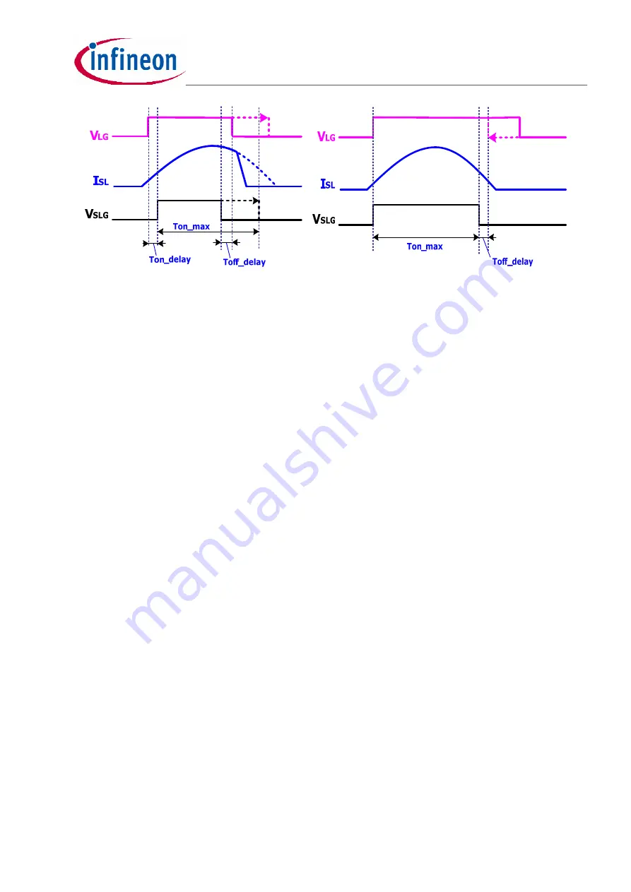
Figure 12
Waveforms for LLC converter with
sw
f
>
r
f
(left) and
sw
f
<
r
f
(right)
2.4.5 SR
Protections
As the SR control in ICE2HS01G is realized with indirect method, there are some cases that the SR can
not work properly. In this cases, the SR gate drive will be disabled. Once the condition is over, IC will
restart the SR with SRSoftstart.
During softstart, the SR is disabled.When the softstart pin voltage is higher than 1.9V for 20ms, SR will be
enabled with SRSoftstart.
When LOAD pin voltage is lower than 0.2V, IC will disable the SR immediately. If LOAD pin voltage is
higher than 0.7V, IC will resume SR with SRSoftstart.
During over-current protection phase, if the softstart pin voltage is lower than 1.8V, SR will be disabled.
The SR will resume with softstart 10ms after SS pin voltage is higher than 1.9V again.
In over-current protection, if the CS pin voltage is higher than 0.9V, SR is disabled. SR will be enabled
with SRSoftstart after CS pin voltage is lower than 0.6V.
All the above four conditions are built inside the IC. If IC detects such a condition, IC will disable SR and
pull down the voltage on SRD pin to zero.
When the CS voltage suddenly drops from 0.55V to below 0.30V within 1ms, the SR gate is turned off for
1ms, after 1ms, SR operation is enabled again with SRsoftstart.
If some fault conditions are not reflected on the four conditions mentioned above but can be detected
outside with other measures, the SR can also be disabled and enabled with softstart from outside. This is
implemented on SRD pin as well. The internal SRD reference voltage has limited current source
capability. If a transistor QSRD is connected as shown in typical application circuit, the voltage on SRD
pin can be pulled to zero if this transistor is turned on, which will stop the SR. If the SRD voltage is
released and increases above 1.75V, SR is enabled with softstart.
2.5 Design
summary
Figure 13 and 14 show the final schematic for the power stage and control circuit for the 300W LLC
converter.