


Application Note
8 of 23
V 1.1
2020-11-09
CoolGaN™ 600 V half-bridge evaluation platform featuring GaN
EiceDRIVER™
Circuit description
3.4
Half-bridge output circuit
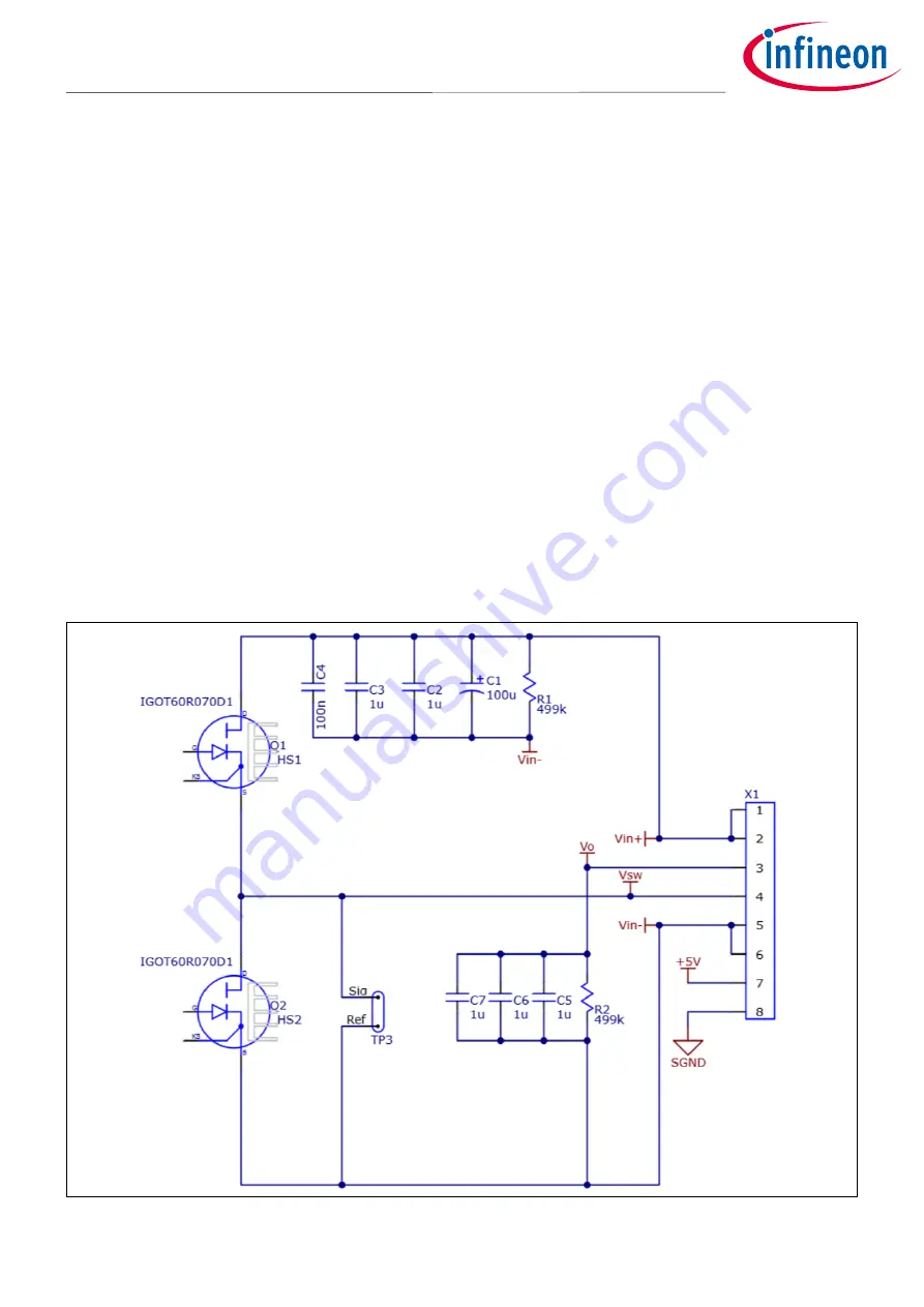
GaN transistors Q1 and Q2 form the high and low-side transistors of the half-bridge, as shown in
. The
drain of Q1 is connected to the DC bus (V
in+
). Capacitors C2, 3, 4 are high-frequency ceramic bypass capacitors,
and C1 is the bulk electrolytic bus capacitor. This capacitive network along with a low-inductance power-loop
layout provides an extremely low-impedance bus with very little overshoot or ringing, as evidenced by the
waveforms in
, where you can see 30 A commutating to the bus in a few ns, with less than 50 V
overshoot. R1 is a bleeder resistor that drains the bus capacitor charge when the circuit is disconnected from a
power supply.
Attention:
Normally the bus capacitor is discharged when the lab power supply is switched-off. But if
the power connector is removed while the capacitor is charged (not recommended!), the bus
capacitor can store high voltage and takes several minutes to dissipate. Be sure to wait until
the capacitor voltage is at a safe level before handling the board.
There is a second DC bus labeled “V
o
.” It is intended to be used as the output bus when the circuit is configured
as a buck converter. It provides a convenient way to connect the inductor back to a low-impedance DC bus and
minimize high-frequency voltage ripple due to the inductor ripple current. The V
o
bus also has a bleed-down
resistor to drain the bus capacitors when it is disconnected. See
for the connections in this mode.
The evaluation board can also be configured for boost-mode operation. In that case, V
o
becomes the input
voltage, and V
in+
becomes the output bus. See section 4.2.3 for complete details.
Figure 7
Half-bridge output circuit