


QUICK START GUIDE
Demonstration System EPC9126xx
EPC – THE LEADER IN GaN TECHNOLOGY |
WWW.EPC-CO.COM
| COPYRIGHT 2019 | | 4
The recommended use of the interposer is the following:
1. Apply solder paste to the U2 pads on the EPC9126xx PCB.
2. Apply solder paste to the appropriate pads on the top side of the
interposer.
3. Carefully position the desired interposer with the bottom side facing
the top side of the EPC9126xx on the U2 footprint.
4. Position the laser diode or desired load on the interposer.
5. Reflow with the recommended temperature profile for the solder
used. The use of a reflow oven that can meet the recommended
soldering specifications is highly recommended. Other reflow
methods may also be used based on the experience of the user.
The power loop inductance, including that of the laser diode, is a primary
factor that determines the shape of the laser pulse. Considerable effort
has been made to minimize power loop inductance while maximizing
the choice of laser diode and its orientation. The discharge caps,
current sense resistors, and the eGaN FET must all be mounted in close
proximity to minimize inductance. As a result, the user must take care
not to damage any components when mounting the laser or changing
other components in the power loop.
Laser diode current pulses can result in peak powers of several hundred
watts to over 1 kW. Laser diodes for lidar applications are designed with
this in mind, but thermal limitations of the laser package mean that
pulse widths, duty cycles, and pulse repetition frequency limitations
must be observed. Read laser diode data sheets carefully and follow any
manufacturers’ recommendations.
This board has been tested with the following laser diodes:
TPGAD1S09H from Excelitas (
http://www.excelitas.com
).
MEASUREMENT CONSIDERATIONS
SMA jacks are provided to measure several voltages in the circuit, including
gate drive input, Q1 gate voltage, Q1 drain voltage, charge voltage of
the energy storage cap, and the sense voltage of the discharge cap
current measurement shunt. All measurement points are designed to be
terminated in 50 Ω, hence when viewing waveforms, the oscilloscope
inputs should be set to a 50 Ω input. Ideally, unused inputs should be
also terminated with a 50 Ω load to prevent the probes from creating
additional resonances. The Q1 drain voltage and the discharge cap sense
voltage have on-board terminations to greatly reduce this effect, and in
practice, the remaining resonances may be small or otherwise tolerable.
It is recommended that the user verify this for their own requirements.
All sense measurement SMAs, except for the shunt measurement, use the
transmission line probe principle to obtain waveform fidelity at sub-ns
time scales. They have been verified to produce near-identical results to a
Tektronix P9158 3 GHz transmission line probe. As a result of their design,
they have a built-in attenuation factor. In addition, the impedance of the
probes is relatively small, and as a result, the test points for high voltage
measurements include a DC blocking capacitor. If long pulse widths are
used, these test points may yield erroneous results, and an external probe
should be used.
The current shunt is designed to estimate the discharge capacitor current.
Substantial effort has been made to reduce the inductive effects of the
current shunt, both through the use of carefully selected resistors and a
compensation network to help compensate for the shunt equivalent
series resistance. However, the shunt is a compromise between current
measurement accuracy and minimizing the impact on the laser driver
performance. If a more accurate shunt waveform measurement is desired,
the shunt resistors may be replaced with ones that provide higher accuracy.
This is likely to require higher resistor values, which can contribute to errors
in the capacitor voltage measurement and in increased power dissipation.
Finally, note that the capacitor current also includes the current due to D1
and D2 (if included), and PCB capacitance.
Table 2 summarizes the properties of the SMA test points for ease of
reference.
Table 2: Properties of SMA test points
Designator
PCB label
Description
Attenuation factor
DC blocking cap LF time constant
Internal 50 Ω
termination
J3
CAP
Discharge capacitor voltage
(VCHARGE on schematic)
41 V/V
10 nF
10 μs
YES
J6
SHUNT
Discharge shunt voltage
21.2 A/V (EPC9126)
45.5 A/V (EPC9126HC)
NO
N/A
NO
J7
V
OUT
Q1 drain voltage
41 V/V
10 nF
10 μs
YES
J9
V
GDIN
Gate drive input
20
NO
N/A
NO
J10
V
GS
Q1 gate voltage
20
NO
N/A
NO
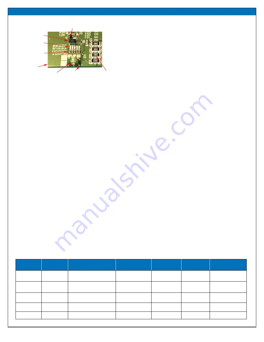
Laser diode
or load
EPC9989
interposer
EPC9126
eGaN FET
Gate driver
Current
shunt
Discharge
capacitors
Recharging
resistors
Figure 5: Laser mounted to EPC9126xx using interposer