


QUICK START GUIDE
Demonstration System EPC9126xx
EPC – THE LEADER IN GaN TECHNOLOGY |
WWW.EPC-CO.COM
| COPYRIGHT 2019 | | 2
DESCRIPTION
The EPC9126 and EPC9126HC development boards are primarily intended
to drive laser diodes with high current pulses with total pulse widths < 3 ns
(half amplitude pulse width). The board is shipped with an EPC2212 or
EPC2001C (HC version) enhancement mode (eGaN®) field effect transistor
(FET). The EPC2212 is an AEC-Q101 automotive qualified 100 V FET capable
of current pulses up to 75 A, and the EPC2001C is a 100 V FET capable
of current pulses up to 150 A. The development boards used the same
printed circuit board with minor component changes in addition to the
different FETs. Due to the fact that the basic design and behavior of the
boards is nearly the same, the term EPC9126xx will be used to refer to either
board, and only when necessary will one or the other board be called
attention to. The EPC9126xx ships with the EPC9989 interposer board.
The EPC9989 has a collection of break-away 5 mm square interposer PCBs
with footprints for different lasers and a collection of other footprints. The
use of the interposers allows many different lasers or other loads to be
mounted while still being able to use the EPC9126xx. The boards do not
include a laser diode, which must be supplied by the user.
The EPC9126xx comprises a ground-referenced eGaN FET driven by a
Texas Instruments LMG1020 gate driver. The EPC9989 interposer provides
multiple options for mounting laser diodes. The printed circuit board is
designed to minimize the power loop inductance while maintaining
mounting flexibility for the laser diode or other load. It includes multiple
on-board passive probes for voltages and discharge capacitor current,
and is equipped with SMA connections for input and sensing designed for
50 ohm measurement systems. In addition, the board includes a narrow
pulse generator capable of sub-nanosecond precision, or the user can
simply send the input to the gate drive directly. Finally, the board can also
be used for other applications requiring a ground-referenced eGaN FET,
e.g. Class E amplifiers or similar. A complete block diagram of the circuit is
given in figure 1, and a detailed schematic in figure 4.
For more information on the EPC2212C or EPC2001C eGaN FETs,
please refer to the datasheets available from EPC at
www.epc-co.com
.
The datasheet should be read in conjunction with this quick start guide.
In addition, there is an application note,
AN027 eGaN FETs for Lidar –
Getting the Most Out of the EPC9126 Laser Driver
. While the note discusses
Rev. 2 of the EPC9126xx, most of the information is applicable to Rev. 3.
SETUP AND OPERATION
Development board EPC9126xx is easy to set up to evaluate the
performance of the EPC2212 or EPC2001C(HC version) eGaN FET. Refer
to Figure 2 for proper connect and measurement setup and follow the
procedure below:
1.
Review laser safety considerations. Observe all necessary laser
safety requirements including the use of personal protection
equipment (PPE) as required. Refer to qualified safety personnel
as necessary.
2. With power off, install laser diode U2 or other load. The use of one
of the interposers from the included EPC9989 be used to mount the
laser or other load, and this is discussed in the section Laser Diode and
Load Considerations for further information.
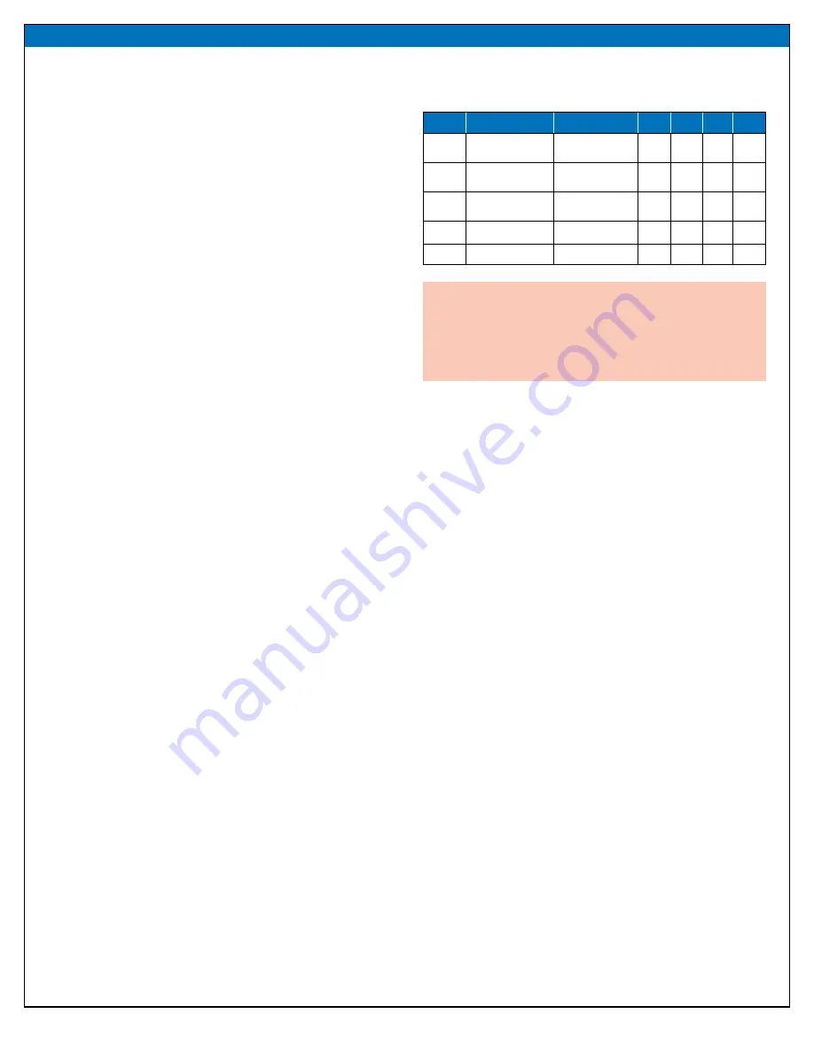
Table 1: Performance Summary (T
A
= 25°C) EPC9126 and EPC9126HC
Symbol
Parameter
Conditions
Min
Nom Max Units
V
Logic
Gate drive and
logic supply
6
12
V
V
BUS
Bus Input
Voltage Range
0
80
V
Z
IN
Input impedance
50
Ω
V
INPUT
Input pulse range
0
5
V
T
Pin
Input pulse width
1
ns
3. With power off, connect the input power supply bus to +V
BUS
(J2)
and ground / return to –V
BUS
(J2) or GND.
4. With power off, connect the logic supply (7-12 V VDC) to +V
Logic
or
GND.
5. With power off, connect the signal pulse generator to the input
J5. J5 is terminated with 50 Ω on the EPC9126, and is designed
for a 5 V logic input. The signal input can handle up to 0.25 W
RMS (3.5 V RMS), which corresponds to a 50% duty cycle at 5 V.
This pulse specification is for the input only, and the user will have
to make informed choices regarding the rest of the circuit.
6. Connect the remaining measurement SMA outputs to an
oscilloscope, using 50 Ω cables and with the scope inputs set
to 50 Ω impedance. See section Measurement Considerations
for more information, including the attenuation values for each
output.
7. Turn on the logic supply voltage to a value within the
specifications.
8. Turn on the bus voltage to a value within the specification.
9. Turn on the pulse source and observe switching operation via the
outputs and any additional desired probing. Laser diode output
may be observed with an appropriate electro-optical receiver.
10. Once operational, adjust the bus voltage, input pulse width, and
pulse repletion frequency (PRF) as desired within the operating
range and observe the system behavior.
11. For shutdown, please follow steps in reverse.
NOTE
: When measuring the high frequency content switch node, care must be taken
to avoid long ground leads. Measure the switch node by placing the oscilloscope
probe tip through the large via on the switch node (designed for this purpose) and
grounding the probe directly across the GND terminal provided. See Figure 3 for
proper scope probe technique.
SAFETY WARNING
: This board is capable of driving laser diodes to
generate high peak power optical pulses. Such pulses are capable of
creating PERMANENT VISION DAMAGE. Laser diodes may emit infrared
(IR) light that is invisible, but which can still cause PERMANENT VISION
DAMAGE. User is fully responsible for following proper laser safety
procedures to prevent vision damage.