


Rev. 1.21
1�8
�ove��e� ��� 2�1�
Rev. 1.21
1��
�ove��e� ��� 2�1�
HT66F488/HT66F489
A/D Flash MCU with EEPROM
HT66F488/HT66F489
A/D Flash MCU with EEPROM
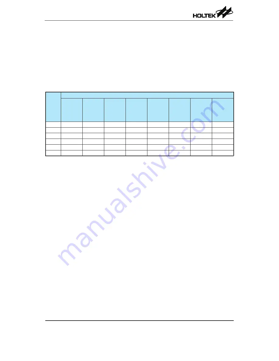
Although the A/D clock source is determined by the system clock f
SYS
, and by bits ADCK2~ADCK0,
there are some limitations on the A/D clock source speed range that can be selected. As the
recommended range of permissible A/D clock period, t
AD
, is from 0.5μs to 10μs, care must be taken
for system clock frequencies. For example, if the system clock operates at a frequency of 4MHz, the
ADCK2~ADCK0 bits should not be set to 000B or 110B. Doing so will give A/D clock periods that
are less than the minimum A/D clock period or greater than the maximum A/D clock period which
may result in inaccurate A/D conversion values.
Refer to the following table for examples, where values marked with an asterisk * show where,
depending upon the device, special care must be taken, as the values may be less than the specified
minimum A/D Clock Period.
f
SYS
A/D Clock Period (t
AD
)
ADCK2,
ADCK1,
ADCK0
=000
(f
SYS
)
ADCK2,
ADCK1,
ADCK0
=001
(f
SYS
/2)
ADCK2,
ADCK1,
ADCK0
=010
(f
SYS
/4)
ADCK2,
ADCK1,
ADCK0
=011
(f
SYS
/8)
ADCK2,
ADCK1,
ADCK0
=100
(f
SYS
/16)
ADCK2,
ADCK1,
ADCK0
=101
(f
SYS
/32)
ADCK2,
ADCK1,
ADCK0
=110
(f
SYS
/64)
ADCK2,
ADCK1,
ADCK0
=111
1MHz
1μs
2μs
4μs
8μs
16μs*
32μs*
64μs*
Undefined
2MHz
5��ns
1μs
2μs
4μs
8μs
16μs*
32μs*
Undefined
4MHz
250ns*
5��ns
1μs
2μs
4μs
8μs
16μs*
Undefined
8MHz
125ns*
250ns*
5��ns
1μs
2μs
4μs
8μs
Undefined
12MHz
83ns*
167ns*
333ns*
66�ns
1.33μs
2.67μs
5.33μs
Undefined
16MHz
62ns*
125ns*
250ns*
5��ns
1μs
2μs
4μs
Undefined
A/D Clock Period Examples
Controlling the power on/off function of the A/D converter circuitry is implemented using the
ADOFF bit in the ADCR0 register. This bit must be zero to power on the A/D converter. When the
ADOFF bit is cleared to zero to power on the A/D converter internal circuitry a certain delay, as
indicated in the timing diagram, must be allowed before an A/D conversion is initiated. Even if no
pins are selected for use as A/D inputs by clearing the ACE7~ACE0 bits in the ACERL registers, if
the ADOFF bit is zero then some power will still be consumed. In power conscious applications it
is therefore recommended that the ADOFF is set high to reduce power consumption when the A/D
converter function is not being used.
The reference voltage supply to the A/D Converter can be supplied from either the positive power
supply pin, AVDD, or from an external reference source supplied on pin VREF. The desired
selection is made using the VREFS bit. As the pin is pin-shared with other function, when the VREF
pin function is selected, then the other pin functions will be disabled automatically.