background image

4. POWER STAGE

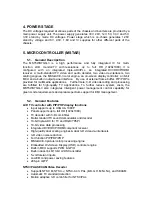
The DC voltages required at various parts of the chassis and inverters are provided by a 
main power supply unit. The power supply generates 33V, 24V, 12V, 5V, 3,3V and 5V, 
3,3V stand by mode DC voltages. Power stage which is on-chasis generates 1,26V
stand by voltage and 8V, 2,6V, 1,8V and 1V supplies for other different parts of the 
chassis.

5. MICROCONTROLLER (MSTAR)

5.1.

General Descripction

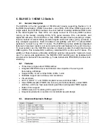
The  MST6WB7GQ-3  is  a  high  performance  and  fully  integrated  IC  for  multi-
function  LCD  monitor/TV  with resolutions  up  to  full  HD  (1920x1080). It  is 
configured  with  an  integrated  triple-ADC/PLL,  an  integrated DVI/HDCP/HDMI 
receiver, a multi-standard TV video and audio decoder, two video de-interlacers, two 
scaling engines, the MStarACE-3 color engine, an on-screen display controller, an 8-bit 
MCU and a built-in output panel interface.    By use of external frame buffer, PIP/POP is 
provided for multimedia applications.    Furthermore, 3-D video decoding and processing 
are fulfilled for high-quality TV applications. To further reduce system costs, the  
MST6WB7GQ-3  also  integrates  intelligent  power  management  control  capability  for  
green-mode requirements and spread-spectrum support for EMI management.

5.2.

General Features

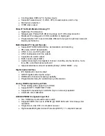
LCD TV controller with PIP/POP display functions

x

Input supports up to UXGA & 1080P

x

Panel supports up to full HD (1920x1080)

x

TV decoder with 3-D comb filter

x

Multi-standard TV sound demodulator and decoder

x

10-bit triple-ADC for TV and RGB/YPbPr

x

10-bit video data processing

x

Integrated DVI/HDCP/HDMI compliant receiver

x

High-quality dual scaling engines & dual 3-D video de-interlacers

x

3-D video noise reduction

x

Full function PIP/PBP/POP

x

MStarACE-3 picture/color processing engine

x

Embedded On-Screen Display (OSD) controler engine

x

Built-in MCU supports PWM & GPIO

x

Built-in dual-link 8/10-bit LVDS transmitter

x

5-volt tolerant inputs

x

Low EMI and power saving features

x

296-pin LQFP

NTSC/PAL/SECAM Video Decoder

x

Supports NTSC M, NTSC-J, NTSC-4.43, PAL (B,D,G,H,M,N,I,Nc), and SECAM

x

Automatic TV standard detection

x

Motion adaptive 3-D comb filter for NTSC/PAL

Содержание L26HP03E

Страница 1: ...cherheitshinweise und Hinweise zur Produktsicherheit in diesem Wartungshandbuch zu lesen SERVICE MANUAL MANUEL D ENTRETIEN WARTUNGSHANDBUCH Data contained within this Service manual is subject to alteration for improvement Les données fournies dans le présent manuel d entretien peuvent faire l objet de modifications en vue de perfectionner le produit Die in diesem Wartungshandbuch enthaltenen Spez...

Страница 2: ...te Maximum Ratings 13 6 4 Pinning 14 7 QAM DEMODULATOR STV0297E 15 7 1 General Desription 15 7 2 Features 16 7 3 Absolute Maximum Ratings 16 7 4 Pinning 17 8 HY5DV281622DT 5 DDR SDRAM 128M 17 8 1 General Description 17 8 2 Features 18 8 3 Absolute Maximum Ratings 18 8 4 Pinning 19 9 IS42S16100C1 SDRAM 19 9 1 General Description 19 9 2 Features 19 9 3 Pinning 20 10 SAW FILTER 20 10 1 IF Filter for ...

Страница 3: ...eneral Description 35 15 1 2 Features 35 15 1 3 Applications 35 15 1 4 Absolute Maximum Ratings 35 15 1 5 Pinning 36 15 2 74HCT4053 36 15 2 1 General Description 36 15 2 2 Features 36 15 2 3 Applications 36 15 2 4 Absolute Maximum Ratings 37 15 2 5 Pinning 37 15 3 NUP4004M5 37 15 3 1 General Description 37 15 3 2 Features 38 15 3 3 Absolute Maximum Ratings 38 15 3 4 Pinning 38 15 4 FDN336P 39 15 4...

Страница 4: ...1 General Description 47 15 11 2 Features 47 15 11 3 Absolute Maximum Ratings 47 15 11 4 Pinning 48 15 12 74LCX245 48 15 12 1 General Description 48 15 12 2 Features 48 15 12 3 Absolute Maximum Ratings 49 15 12 4 Pinning 49 15 13 FSA3157 49 15 13 1 General Description 49 15 13 2 Features 50 15 13 3 Absolute Maximum Ratings 50 15 13 4 Pinning 50 15 14 FMS6145 51 15 14 1 General Description 51 15 14...

Страница 5: ...GS 59 16 1 Video Setup 59 16 2 AudioSetup 59 16 3 Service Scan Tuning Setup 61 16 4 Options 62 16 5 External Source Settings 64 16 6 Preset 64 16 7 NVM Edit 64 16 8 Programming 64 16 9 Diagnostic 65 16 10 Product Info 65 17 SOFTWARE UPDATE DESCRIPTION 65 16 1 17MB35 Analog Part Software Update With Bootloader Procedure 65 16 2 17MB30 HDCP key upload procedure 68 16 3 17MB35 Digital Software Update...

Страница 6: ......

Страница 7: ...Stereo audio input for PC Common 1 Line out Common 1 Subwoofer out Common 1 S PDIF output Common 1 Side S Video Optional 1 Headphone Common 1 Common interface Optional 1 Digital USB Opional 1 Analog USB Opional 1 RS232 Optional 1 Smart card connector Optional 2 TUNER A horizontal mounted and Digital Half Nim tuner is used in the product which covers 3 Bands From 48MHz to 862MHz for COFDM from 45 2...

Страница 8: ...grated audio amplifiers which dramatically reduces solution size by integrating the following x 180m SRZHU 026 7V x Startup Shutdown pop elimination x Short circuit protection x Mute Standby The MP7722 utilizes a single ended output structure capable of delivering 2 x 20W into 4 speakers MPS Class D Audio Amplifiers exhibit the high fidelity of a Class A B amplifier at efficiencies greater than 90...

Страница 9: ...ination Circuit x Thermal and Short Circuit Protection x Integrated 180m 6ZLWFKHV x Mute Standby Modes Sleep x Thermally Enhanced 20 Pin TSSOP Package with Exposed Pad 3 3 Applications x Surround Sound DVD Systems x Televisions x Flat Panel Monitors x Multimedia Computers x Home Stereo Systems 3 4 Absolute Ratings 3 4 1 Electrical Characteristics ...

Страница 10: ...3 4 2 Operating Specifications 3 5 Pinning ...

Страница 11: ...processing are fulfilled for high quality TV applications To further reduce system costs the MST6WB7GQ 3 also integrates intelligent power management control capability for green mode requirements and spread spectrum support for EMI management 5 2 General Features LCD TV controller with PIP POP display functions x Input supports up to UXGA 1080P x Panel supports up to full HD 1920x1080 x TV decode...

Страница 12: ...ut x Built in audio output DAC s x Audio processing for loudspeaker channel including volume balance mute tone EQ and virtual stereo surround x Optional advanced surround available Dolby1 SRS2 BBE3 etc Digital Audio Interface x I2S digital audio input output x S PDIF digital audio input output x HDMI audio channel processing capability x Programmable delay for audio video synchronization Analog RG...

Страница 13: ...d consumer To lower system cost the SiI9185A provides a complete solution for switching sink side HDMI signals This includes DDC switching individual HPD control and 5V sense The addition of these features eliminates additional external components helping to lower cost For source side applications the SiI9185A DDC switching can be bypassed with an external 4 channel I2C bus switch e g Texas Instru...

Страница 14: ...6 4 Pinning Configuration Pins ...

Страница 15: ...G 4 block processing of QAM signals It is intended for the digital transmission of compressed television sound and data services over cable It is fully compliant with ITU T J83 Annexes A C or DVB C specification bitstreams ETS 300 429 Digital broadcasting systems for television sound and data services Framing structure channel coding and modulation Cable Systems It can handle square 16 64 256 QAM ...

Страница 16: ...t IF architecture in all QAM quadrature amplitude modulation modes x Supports 16 32 64 128 and 256 point constellations x Small footprint package 10 x 10 mm x Very low power consumption x Full digital demodulation x Variable symbol rates x Front derotator for better low symbol rate performance and relaxed tuner constraints x Integrated matched filtering x Robust integrated adaptive pre and post eq...

Страница 17: ... SDRAMs offer fully synchronous operations referenced to both rising and falling edges of the clock While all addresses and control inputs are latched on the rising edges of the CK falling edges of the CK Data Data strobes and Write data masks inputs are sampled on both rising and falling edges of it The data paths are internally pipelined and 2 bit prefetched to achieve very high bandwidth All in...

Страница 18: ... DQS centers when write centered DQ x Data DQ and Write masks DM latched on the both rising and falling edges of the data strobe x All addresses and control inputs except Data Data strobes and Data masks latched on the rising edges of the clock x Write mask byte controls by LDM and UDM x Programmable CAS latency 3 4 supported x Programmable Burst Length 2 4 8 with both sequential and interleave mo...

Страница 19: ...improved performance The synchronous DRAMs achieve high speed data transfer using pipeline architecture All inputs and outputs signals refer to the rising edge of the clock input 9 2 Features x Clock frequency 200 166 143 MHz x Fully synchronous all signals referenced to a positive clock edge x Two banks can be operated simultaneously and independently ...

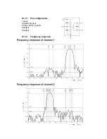
Страница 20: ...capability x Burst termination by burst stop and precharge command x Byte controlled by LDQM and UDQM x Industrial temperature up to 143 MHz x Packages 400 mil 50 pin TSOP II 60 ball fBGA x Lead free package option 9 3 Pinning 10 SAW FILTER 10 1 IF Filter for Audio Applications Epcos K9656M 10 1 1 Standart x B G x D K x I x L L 10 1 2 Features x TV IF audio filter with two channels x Channel 1 L w...

Страница 21: ...10 1 3 Pin configuration 1 Input 2 Switching input 3 Chip carrier ground 4 Output 5 Output 10 1 4 Frequency response ...

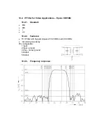
Страница 22: ...58M 10 2 1 Standart x B G x D K x I x L L 10 2 2 Features x TV IF filter with Nyquist slopes at 33 90 MHz and 38 90 MHz x Constant group delay Pin configuration 1 Input 2 Input ground 3 Chip carrier ground 4 Output 5 Output 10 2 3 Frequency response ...

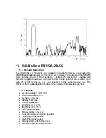
Страница 23: ...ation are essential Up to eight HT24LC01 02 devices may be connected to the same two wire bus The HT24LC01 02 is guaranteed for 1M erase write cycles and 40 year data retention 11 2 Features x Operating voltage 2 4V 5 5V x Low power consumption x Operation 5mA max x Standby 5mA max x Internal organization x 1K HT24LC01 128 8 x 2K HT24LC02 256 8 x 2 wire serial interface x Write cycle time 5ms max ...

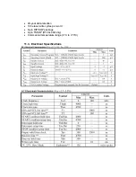
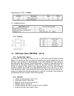
Страница 24: ...x 40 year data retention x 106 erase write cycles per word x 8 pin DIP SOP package x 8 pin TSSOP HT24LC02 only x Commerical temperature range 0 C to 70 C 11 3 Electrical Specifications ...

Страница 25: ...ta that changes frequently The 24C32 is capable of both random and sequential reads up to the 32K boundary Functional address lines allow up to eight 24C32 devices on the same bus for up to 256K bits address space Advanced CMOS technology makes this device ideal for low power non volatile code and data applications The 24C32 is available in the standard 8 pin plastic DIP and 8 pin surface mount SO...

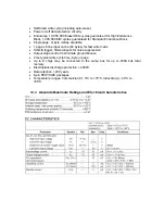
Страница 26: ...e 64 bytes for fast write loads x Schmitt trigger filtered inputs for noise suppression x Output slope control to eliminate ground bounce x 2 ms typical write cycle time byte or page x Up to 8 chips may be connected to the same bus for up to 256K bits total memory x Electrostatic discharge protection 4000V x Data retention 200 years x 8 pin PDIP SOIC packages x Temperature ranges Commercial C 0 C ...

Страница 27: ...12 4 Pinning ...

Страница 28: ...ice is not in operation and CS is high it is put in standby mode and draws less than 10uA DC current The MX25L512 utilize MXIC s proprietary memory cell which reliably stores memory contents even after 100 000 program and erase cycles 13 2 Features GENERAL x Serial Peripheral Interface SPI compatible Mode 0 and Mode 3 x 524 288 x 1 bit structure x 16 Equal Sectors with 4K byte each x Any Sector ca...

Страница 29: ...e by an internal algorithm that automatically times the program pulse widths Any page to be programed should have page in the erased state first x Status Register Feature x Electronic Identification x JEDEC 2 byte Device ID x RES command 1 byte Device ID HARDWARE FEATURES x SCLK Input x Serial clock input x SI Input x Serial Data Input x SO Output x Serial Data Output x WP pin x Hardware write pro...

Страница 30: ...n Compared with Cheertek s previous generations of STB receiver devices CT216T further interates COFDM demodulator USB 2 0 HS host controller memory card reader 1 2 bit SPIFlash interface audio DAC PWM in out and SAR ADC functions In additiont special enhangements are provided such as MPEG 4 video decoding 16 bit OSD with anti ...

Страница 31: ...rsion detection x Integrated ADC x Direct IF 36 167 MHz or 43 75 MHz or low IF 4 57 MHz supported x Single IF AGC or dual RF lF AGC controls with ǻȈ modulabon x Impulsive noise cancellation x Carrier acquisition range 400 kHz extensible to 600 kHz in 8MHz BW x Adjacent channel interference ACI filter for supporting 6 7 and 8MHz channels with one 8MHz analog filter x Co channel interterence CCl sup...

Страница 32: ...KHz x SPDIF out for AC 3 by pass x Embedded 2 channels audio DAC for L R outputs x Digital mute control and volume adjustment OSD On Screen Display x There are total 9 display planes border background video RS1 Rectangle Strip 1 RS2 OSD RS3 RS4 and cursor x 4 8l16 bit OSD with anti flickering and anti flutter x Support alpha blending per color x Adjustable brightness control in window x Bitmap OSD...

Страница 33: ...T with 16 byte FIFO x 2 wire serial 2WS in master mode x Up to 2 IS0 7816 compliant SC 1 in 128 pin can also be used as UART x 5 digits 7 Segrnent LED control x 5x3 two dimension key scan x 2 SAR ADC input x 4 PWM input output x 1 HW IR command decode x GPIO Electrical and Physical Characteristics x Capable of using single 27MHz clock input crystal x 1 8V and 3 3V dual power supply x Power standby...

Страница 34: ......

Страница 35: ...output voltage accuracy to within 1 The LM1117 series is available in SOT 223 TO 220 and TO 252 D PAK pDFNDJHV PLQLPXP RI ȝ tantalum capacitor is required at the output to improve the transient response and stability 15 1 2 Features x Available in 1 8V 2 5V 2 85V 3 3V 5V and Adjustable Versions x Space Saving SOT 223 Package x Current Limiting and Thermal Protection x Output Current 800mA x Line R...

Страница 36: ... The VCC to GND ranges are 2 0 V to 10 0 V for 74HC4053 and 4 5 V to 5 5 V for 74HCT4053 The analog inputs outputs nY0 and nY1 and nZ can swing between VCC as a positive limit and VEE as a negative limit VCC VEE may not exceed 10 0 V For operation as a digital multiplexer demultiplexer VEE is connected to GND typically ground 15 2 2 Features x Low ON resistance x 80 W typical at VCC VEE 4 5 V x 70...

Страница 37: ...2 5 Pinning 15 3 NUP4004M5 15 3 1 General Description This 5 Pin bi directional transient suppressor array is designed for applications requiring transient overvoltage protection capability It is intended for use in transient voltage and ...

Страница 38: ... is ideal for situations where board space is a premium 15 3 2 Features x Bi directional Protection for Four Lines in a Single TSOP 5 Package x Low Leakage Current x Low Capacitance x Provides ESD Protection for JEDEC Standards JESD22 x Machine Model Class C x Human Body Model Class 3B x Provides ESD Protection for IEC 61000 4 2 15 kV Air 8 kV Contact x This is a Pb Free Device 15 3 3 Absolute Max...

Страница 39: ... switch from the I2C bidirectional mode to the Transmit Only mode except when the power supply is removed The device operates with a power supply value as low as 2 5V Both Plastic Dual in Line and Plastic Small Outline packages are available 15 4 2 Features x 1 MILLION ERASE WRITE CYCLES x 40 YEARS DATA RETENTION x 2 5V to 5 5V SINGLE SUPPLY VOLTAGE x 400k Hz COMPATIBILITY OVER the FULL RANGE of S...

Страница 40: ... 200 μA Per Amplifier x Wide Common Mode and Differential Voltage Ranges x Low Input Bias and Offset Currents x Common Mode Input Voltage Range Includes VCC x Output Short Circuit Protection x High Input Impedance JFET Input Stage x Internal Frequency Compensation x Latch Up Free Operation x High Slew Rate 3 5 V μs Typ 15 5 3 Absolute Maximum Ratings ...

Страница 41: ...tionally high current capability which is far greater than most analog switches offered today A single 5V supply is all that is required for operation The PI5V330 offers a high performance low cost solution to switch between video sources The application section describes the PI5V330 replacing the HC4053 multiplier and buffer amplifier 15 6 2 Features x High performance low cost solution to switch...

Страница 42: ...ons the steering diodes direct the transient to either the power supply line or to the ground line The internal unique design of clamping cell prevents over voltage on the power line protecting any downstream components AZC099 04S may be used to meet the ESD immunity requirements of IEC 61000 4 2 Level 4 15kV air 8kV contact discharge 15 7 2 Features x ESD Protect for 4 high speed I O channels x P...

Страница 43: ... WLCSP8 The device is fabricated in a 1 mm Complementary Metal Oxide Semiconductor CMOS process and has been primarily developed for portable digital audio applications The difference between the TDA1308 and the TDA1308A is that the TDA1308A can be used at low supply voltages 15 8 2 Features x Wide temperature range x No switch ON OFF clicks x Excellent power supply ripple rejection x Low power co...

Страница 44: ... 0 1mF standard external capacitors for operating from 3V supply The ST3222 has two receivers and two drivers The ST3222 features a 1mA shutdown mode that reduces power consumption and extends battery life in portable systems Its receivers can remain active in shutdown mode allowing external devices such as modems to be monitored using only 1mA supply current The device is guaranteed to run at dat...

Страница 45: ...Ratings 15 9 4 Pinning 15 10 LM358D 15 10 1 General Description The LM158 series consists of two independent high gain internally frequency compensated operational amplifiers which were designed specifically to operate from a ...

Страница 46: ...e electronics without requiring the additional 15V power supplies The LM358 and LM2904 are available in a chip sized package 8 Bump micro SMD using National s micro SMD package technology 15 10 2 Features x Available in 8 Bump micro SMD chip sized package x Internally frequency compensated for unity gain x Large dc voltage gain 100 dB x Wide bandwidth unity gain 1 MHz temperature compensated x Wid...

Страница 47: ...is fabricated with an advanced CMOS technology to achieve high speed operation while maintaining CMOS low power dissipation 15 11 2 Features x 5V tolerant inputs and outputs x 2 3V to 3 6V VCC specifications provided x 6 5ns Tpd max VCC 3 3V 10μA ICCmax x Power down high impedance inputs and outputs x Supports live insertion withdrawal x 24mA output drive VCC 3 0V x Implements patented noise EMI r...

Страница 48: ...th the A and B ports by placing them in a high impedance state The LCX245 is fabricated with an advanced CMOS technology to achieve high speed operation while maintaining CMOS low power dissipation 15 12 2 Features x 5V tolerant inputs and outputs x 2 3V to 3 6V VCC specifications provided x 7 0ns tPDmax VCC 3 3V 10μA ICCmax x Power down high impedance inputs and outputs x Supports live insertion ...

Страница 49: ...r de multiplexer bus switch The device is fabricated with advanced sub micron CMOS technology to achieve high speed enable and disable times and low on resistance The break beforemake select circuitry prevents disruption of signals on the B Port due to both switches temporarily being enabled during select pin switching The device is specified to operate over the 1 65 to 5 5V VCC operating range ...

Страница 50: ...urface mount package x Ultra small MicroPak Pb free leadless package x RZ 2Q 5HVLVWDQFH ȍ RQ W SLFDO DW 9 9 x Broad VCC operating range 1 65V to 5 5V x Rail to rail signal handling x Power down high impedance control input x Over voltage tolerance of control input to 7 0V x Break before make enable circuitry x 250 MHz 3dB bandwidth 15 13 3 Absolute Maximum Ratings 15 13 4 Pinning ...

Страница 51: ...upled inputs are required The outputs can drive AC or DC FRXSOHG VLQJOH ȍ RU GXDO ȍ ORDGV FRXSOLQJ WKH outputs removes the need for output coupling capacitors The input DC levels are offset approximately 280mV at the output 15 14 2 Features x Five 4th order 8MHz SD OWHUV x Drives single AC or DC FRXSOHG YLGHR ORDGV 9SS ȍ x Drives dual AC or DC FRXSOHG YLGHR ORDGV 9SS ȍ x Transparent input clamping...

Страница 52: ...r of locations in a programmed sequence Accesses begin with the registration of an ACTIVE command which is then ollowed by a READ or WRITE command The address bits registered coincident with the ACTIVE command are used to select the bank and row to be accessed BA0 BA1 select the bank A0 A11 select the row 15 15 2 Features x PC66 PC100 and PC133 compliant x 143 MHz graphical 4 Meg x 16 option x Ful...

Страница 53: ...on Current mode operation provides fast transient response and eases loop stabilization Fault condition protection includes cycle by cycle current limiting and thermal shutdown Adjustable soft start reduces the stress on the input source at turn on In shutdown mode the regulator draws 20μA of supply current The MP1583 requires a minimum number of readily available external components to complete a...

Страница 54: ... x Up to 95 Efficiency x 20μA Shutdown Mode x Fixed 385KHz frequency x Thermal Shutdown x Cycle by Cycle Over Current Protection x Wide 4 75 to 23V operating Input Range x Output Adjustable From 1 22 to 21V x Under Voltage Lockout x Available in 8 pin SOIC Package x 3A Evaluation Board Available 15 16 3 Absolute Maximum Ratings 15 16 4 Pinning ...

Страница 55: ...o 6V input voltage The output voltage can be regulated as low as 0 6V The MP2112 can also run at 100 duty cycle for low dropout applications The MP2112 is available in a space saving 6 pin QFN package 15 17 2 Features x High Efficiency Up to 95 x 1MHz Constant Switching Frequency x 1A Available Load Current x 2 5V to 6V Input Voltage Range x Output Voltage as Low as 0 6V x 100 Duty Cycle in Dropou...

Страница 56: ...d In Application programming ICP and IAP Endurance 10K write erase cycles guaranteed Data retention 20 years at 55 C 384 bytes RAM 128 bytes data EEPROM with read out protection 300K write erase cycles guaranteed data retention 20 years at 55 C x Clock Reset and Supply Management 3 level low voltage supervisor LVD for main supply and an auxiliary voltage detector AVD for safe power on off Clock so...

Страница 57: ...15 18 4 Pinning ...

Страница 58: ...T output Both devices are available in SOT 23 and SC 70 packages The MAX809 810 are optimized to reject fast transient glitches on the VCC line Low supply current of 0 5 _A VCC 3 2 V makes these devices suitable for battery powered applications 15 19 2 Features x Precision VCC Monitor for 1 5 V 2 5 V 3 0 V 3 3 V and 5 0 V Supplies x Precision Monitoring Voltages from 1 2 V to 4 9 V Available in 10...

Страница 59: ...round item is seen in Feature menu If Yes selected Blue Background is on and not seen in Feature menu Film Mode If Yes selected Film Mode feature is active Dynamic Contrast If Yes selected Dynamic Contrast feature is active Game Mode If Yes selected Game Mode feature is active SRGB For PC If Yes selected PCs can use SRGB option Dynamic Noise Reduction If Yes selected Dynamic Noise Reduction featur...

Страница 60: ...Noise Reduction Time Value between 0 to 15 AVL Attack Time Value between 0 to 255 AVL Release Time Value between 0 to 255 Prescales AVL On FM Prescale Value between 0 to 255 AM Prescale Value between 0 to 255 NICAM Prescale Value between 0 to 255 SCART Prescale Value between 0 to 255 FAV Prescale Value between 0 to 255 DTV Prescale Value between 0 to 255 HDMI Prescale Value between 0 to 255 YPbPr ...

Страница 61: ...T Clipping Value between 0 to 255 FAV Clipping Value between 0 to 255 DTV Clipping Value between 0 to 255 HDMI Clipping Value between 0 to 255 YPbPr PC Clipping Value between 0 to 255 An USB Clipping Value between 0 to 255 Dig USB Clipping Value between 0 to 255 16 3 Service Scan Tuning Setup First Search for L L ATS Delay Time ms Value between 0 to 200 Main Tuner Setup Tuner Type LC_TDTC_GXX1D Th...

Страница 62: ...n the USB Files Options 2 Source List menu If Yes selected Sorce List Menu appears on the screen when press source button RS232 for B2B If Yes selected Remote Control commandsthe TV via RS232 and vice versa RC Select RC Group 1 RC Group 2 RC Group 3 RC Group 4 RC Group 5 RC Group 6 Double Digit Key If Yes selected Double Digit Button on RC activates Protection If Yes selected short circuit protect...

Страница 63: ... Teletext subtitles can be seen Optional Features Default Zoom Menu 16 9 4 3 Panaromic 14 9 Zoom Menu Timeout Menu 15 Sec 30 Sec 60 Sec No Time Backlight If Yes selected Backlight feature is active 100 Step Slider If Yes selected 64 step sliders will become 100 step sliders Analog USB Enabled If Yes selected Analog USB option is active Menu Double Size If Yes selected menu sizes increases CEC Enab...

Страница 64: ...DMI 1 HDMI 2 HDMI 3 HDMI 4 YPbPr PC 16 6 Preset User Ad j ADC Adj Service Adj All Adj Init Factory Channels 16 7 NVM Edit NVM edit addr hex NVM edit data hex NVM data dec 16 8 Programming HDMI DDC Update Mode HDCP Key Update Mode Software Bypass If On selected speaker effects are bypassed LVDS Clock Step Value between 0 to 255 Memory Clock Step Value between 0 to 255 DTV Download If On selected DT...

Страница 65: ... to be any times of 64 Kb 4 The Test Binary File It has tin extension and it is used and written by the test groups It is run to understand the problem part of the hardware Alltough a file that is used by the bootloader can be had any one of these extensions its name has to be VESTEL_S and it has to be located in the root directory of the usb device 1 2 Usage of The Bootloader 1 The starting to pa...

Страница 66: ...d File menu item and choosing 1K Xmodem from protocol section Figure 1 The Sample Output Before Sending The File 2 EEProm update To Update eeprom content via uart scart dsub9 or i2c with Mstar tool can used Serial connection settings are listed below Bit per second 9600 Data bits 8 Parity None Stop bits 1 Flow control None Programming menu item is choosed in the service menu and switch HDCP Key Up...

Страница 67: ...em menu in the hyperterminal To download hdcp key press k or to download eeprom content press w Figure 3 Xmodem Menu If the repeated C characters are seen you can transfer file content via select Transfer Send File and choose Xmodem protocol and click the Send button ...

Страница 68: ...ate 9600 bps Data Bits 8 Stop Bits 1 Parity None Flow Control None 3 Enter service menu by pressing 4 7 2 5 consecutively while main menu is open 4 Select 9 Programming 5 Select HDMI HDCP Update Mode yes 6 On Hyper Terminal Window press k 7 Click on send file under Transfer Tab 8 Select Xmodem and choose the HDCP key to be uploaded 9 Press send button 10 Restart TV set ...

Страница 69: ...gramming step 6 Change 6 DTV Download to On 7 Switch to the Stby mode Adjusting HyperTerminal 1 Connect the MB35 SCART Interface to SCART1 bottom SCART plug 2 Also connect the MB35 SCART Interface to PC 3 Open HyperTerminal 4 Determine the COM settings listed and showed below x Bit per second 115200 x Data bits 8 x Parity None x Stop bits 1 x Flow control None COM Properties Window 6 Click OK ...

Страница 70: ... Mode 3 The Space button on the keyboard must be pressed when the following window can be seen Selection Window 4 Press the 2 button on the keyboard for choosing 2 Upgrade Application with Xmodem 5 Repeating C characters are seen in the HyperTerminal menu The Sample Output Before Sending The File ...

Страница 71: ...l option Selection of File File and Protocol Selection Window Note In the Software updating Procedure section when the first C character is seen the filename selection process must be finished before 10 seconds If the process can not be finished the file sending operation will be cancelled The following figure shows this situation ...

Страница 72: ...Capture of Receving Data Failing 9 When sending the file the following window must be seen Capture of Sending Process 10 After the sending process the following HyperTerminal window must be seen ...

Страница 73: ... repeated from the step X Select the Filename xxxx_slot2 img using Browse 12 After sending the second program file the Software Updating Procedure will be succesful Note After the File Sending Process 1 Upgrade Application with FUM 2 Upgrade Application with Xmodem options must be seen End of The Sending Process ...

Страница 74: ...n the flash and then a system reset is performed 5 After the reset digital module starts with new software Revert operation With revert operation it is possible to downgrade the software Revert operation is very similar to upgrade process In the revert operation file name should be f_up bin Also user confirmation is not asked 1 Copy the bin file into the USB flash memory root directory This file s...

Страница 75: ......

Страница 76: ...18 2 Power Management ...

Страница 77: ...18 3 Integrated DVB T Receiver Block Diagram ...

Страница 78: ...18 4 MSTAR Block Diagram ...

Страница 79: ... 220u 6V3 IDTV_SW 1 TP151 1 2 R503 10K 1 2 L113 1U 1 2 L101 1U 1 2 L111 1U 2 1 1U L114 RF_AGC 1 2 R210 100K 1 2 R209 100K 1 2 F186 330R 1 2 F185 330R 1 2 F184 330R 1 2 F158 330R 1 2 F159 330R 1 2 C600 47U 16V 1 2 C597 220P 50V 1 2 C510 100N 10V 1 2 C467 10U 10V 1 2 C448 47U 16V 1 2 D145 BA782 1 2 R231 3K3 1 2 R474 6K8 1 2 R473 6K8 1 2 S103 RF_AGC_A RF_AGC_A 5V_VCC 5V_TUN 2 1 10K R501 8V_VCC 5V_TUN...

Страница 80: ..._AUD_R_IN 2 1 50V 1N C477 SC1_AUD_L_IN SC1_B 1 2 C104 220P 50V SC1_R RCA_Y 2 1 47R R130 2 1 50V 27P C440 1 2 C441 27P 50V 1 2 C437 27P 50V SC1_G SC1_CVBS_IN S_VIDEO_Y_IN S_VIDEO_C_IN 2 1 50V 220P C110 1 2 F198 600R 1 2 F209 600R SPDIF_OUT_OPTICAL 1 2 3 Q117 BC848B 2 1 600R F196 1 2 3 4 5 6 7 8 9 10 11 12 13 14 15 16 17 18 19 20 21 SC101 1 2 3 IR101 1 2 F211 600R 1 2 F210 600R 2 1 600R F208 2 1 600...

Страница 81: ...0V AVDD_AU 1 2 R131 47R 1 2 C420 47N 16V 9 10 11 12 13 14 15 16 8 7 6 5 4 3 2 1 U129 PI5V330 RIN1P SOGIN1 GIN1P BIN1P VGA_R VGA_HSNC VGA_VSNC 1 2 C151 100N 10V 1 2 C150 100N 10V BIN1P RIN1P GIN1P SOGIN1 BIN0P BIN2P SOGIN2 GIN2P RIN2P C1 Y1 C0 Y0 2 1 16V 47N C416 SW_PR 2 1 S109 2 1 S110 RCA_PR DVB YPBPR_SW 1 2 R627 1K SW_Y 1 2 S108 RCA_Y 2 1 S112 2 1 S107 RCA_PB 1 2 S111 SW_Y SW_PB SOGIN2 GIN2P BIN...

Страница 82: ..._1 HDMIB_C HDMIA_C HDMIA_0 HDMIA_0 AVDD_33 HDMIA_1 HDMIA_1 HDMIA_2 HDMIA_2 AVDD_USB USB_DP CEC CEC 1 2 R631 1K 2 1 R489 47K 2 1 R490 47K 2 1 R485 47K 1 2 R628 1K 2 1 R486 47K 1 2 47K R494 1 2 47K R493 2 1 1K R632 2 1 R492 47K 2 1 R491 47K 2 1 10V 10U C381 1 2 C379 10U 10V 2 1 10V 10U C380 1 2 C169 100N 10V 1 2 R119 910R 2 1 330R F122 1 2 330R F124 1 2 3 Q101 2N7002 1 2 S113 SIDE_HDMI_SDA SIDE_HDMI...

Страница 83: ...UART0_RXD0 UART0_TXD0 TX SDA_SC 1 2 R395 1k USB_OCD VFD_CLK_STBY VFD_DATA_STBY 5V_STBY 1 2 R552 10K 3V3_STBY 1 2 D149 C5V6 VFD_CLK_STBY 5V_STBY 3V3_STBY OVER_CUR_DETECT 1 2 R742 20K 3V3_STBY 2 1 4K7 R279 LED1 1 2 R422 10K 1 2 3 Q131 BC848B 1 2 R531 10K 1 2 R381 220R 1 2 3 Q149 BC858B 1 2 C531 220P 50V 1 2 R234 4K7 1 2 R745 1K 1 2 R421 10K 1 2 D148 C5V6 1 2 R233 4K7 1 2 C530 220P 50V 2 1 100R R353 ...

Страница 84: ...MADR_5 MADR_4 VDDM 1 2 F162 60R VDDM 1 2 C203 100N 10V 1 2 F157 330R 1 2 3 4 5 6 7 8 100R R592 1 2 3 4 5 6 7 8 R590 100R 3V3_STBY 1 2 C500 1N 50V VDD_DMQ 2V6_VCC VDDM MCLK 2 1 330R F125 1 2 C195 100N 10V VDDM VDDM VDDM 2 1 10V 100N C194 VDDM CASZ VDDC VDDC 26 27 28 29 30 31 32 33 34 35 36 37 38 39 40 41 42 43 44 45 46 47 48 49 50 25 24 23 22 21 20 19 18 17 16 15 14 13 12 11 10 9 8 7 6 5 4 3 2 1 U1...

Страница 85: ...2U C527 1 2 C528 22U 50V 1 2 C591 68N 50V 1 2 3 4 5 6 7 8 R245 47R 1 2 C560 390P 50V 12V_VCC 2 1 50V 68N C595 1 2 1N4148 D127 8V_VCC 1 2 C346 1U 16V VDD_AUDIO 2 1 50V 2N2 C539 1 2 C387 10U 10V 1 2 S128 1 2 R729 100K 2 1 10K R541 2 1 50V 22P C582 1 2 C581 22P 50V 1 2 R398 120K 2 1 50V 390P C561 1 2 D118 C5V6 1 2 C594 68N 50V 2 1 50V 68N C596 2 1 50V 1N C505 1 2 R112 12K 2 1 100K R732 1 2 R728 100K ...

Страница 86: ... 6 7 8 R426 33R QAM_TS_D3 QAM_TS_D7 QAM_TS_D6 QAM_TS_D5 QAM_TS_D4 1 2 3 4 5 6 7 8 R429 33R 1 2 3 4 5 6 7 8 R323 47R 1 2 3 4 5 6 7 8 9 10 11 12 13 14 15 16 17 18 19 20 U125 74LCX244 1 2 3 4 5 6 7 8 9 10 11 12 13 14 15 16 17 18 19 20 U108 74LCX245 1 2 3 4 5 6 7 8 R431 33R 1 2 3 4 5 6 7 8 R430 33R 1 2 C280 1U 16V 1 2 C279 1U 16V 1 2 C392 10U 16V 1 2 C224 100N 10V 1 2 C226 100N 10V 1 2 C393 10U 16V 1 ...

Страница 87: ... 7 6 5 4 3 2 1 U139 FMS6145 1 2 C303 1N 1 2 C302 1N 1 2 3 4 5 6 7 8 U116 PI6CX100 27 28 29 30 31 32 33 34 35 36 37 38 39 40 41 42 43 44 45 46 47 48 49 50 51 52 53 54 27 26 25 24 23 22 21 20 19 18 17 16 15 14 13 12 11 10 9 8 7 6 5 4 3 2 1 MT48LC4M16A2TG8E U134 MCLK_SDRAM MCLK_SDRAM MDQM 1 2 3 4 5 6 7 8 R436 33R CAB TER_AGC_SW FUM_EN 1 2 F135 330R 1 2 F136 330R 1 2 C252 100N 10V 1 2 F133 330R 1 2 F1...

Страница 88: ...07 28K7 3V3_VCC 1 2 C535 1N 50V 1 2 C536 1N 50V 1 2 R701 33K 1 2 C519 100N 10V 1 2 C518 100N 2 1 100N C517 2 1 16V 470U C456 1 2 C516 100N 10V 1 2 C470 47U 16V 1 2 C571 22U 16V 1 2 C572 22U 16V 1 2 C578 22U 16V 1 2 C358 10N 16V 1 2 C357 10N 16V 2 1 10V 10U C406 1 2 F169 60R 1 2 F171 60R 1 2 C576 22U 16V 1 2 C575 22U 16V 1 2 C579 22U 16V 1 2 C574 22U 16V 1 2 C573 22U 16V 6 5 4 3 2 1 MP2112 U145 1 2...

Страница 89: ...9 269 268 267 266 265 264 263 262 261 260 259 258 257 256 255 254 253 252 251 250 249 248 247 246 245 244 270 271 U138 MST6WB7GQ 3 1V0_VCC_PIX TX_PIX_A_0_N 2 1 10K R583 1 2 R581 10K 1 2 33R R480 SCL 1 2 33R R481 SDA 2 1 50V 220P C127 1 2 C126 220P 50V 2 1 50V 220P C125 2 1 10V 100N C325 1 2 C415 10U 10V 2 1 10V 10U C414 2V6_VCC 2 1 10V 100N C316 2V6_VCC_PLL 3V3_VCC_PIX 2V6_VCC_PIX 2 1 10V 100N C31...

Страница 90: ...1 3V3_LPW 3V3_LPW 1 2 3 4 5 CN128 3V3_LPW LED1 STBY_ON OFF_NOT ICC_RESET_STBY 2 1 R771 100R 1 2 C615 100n 16V KEYBOARD_STBY_OUT IR_MAIN IR_MAIN 1 2 S201 IR_IN 2 1 220R F221 1 2 C614 100n IR_IN 1 2 S200 ICC_DATA_STBY ICC_CLK_STBY 1 2 F233 600R 29 28 27 26 23 22 21 20 19 18 17 9 10 11 12 13 14 15 16 1 2 3 4 5 6 7 8 32 31 30 24 25 U149 STLITE49M 1 2 3 4 5 6 7 8 R776 33R 1 2 C617 18p 50V 1 2 C616 18p ...

Страница 91: ... GND 7 3V3 6 5V 5 AC_GND 3 NC 2 B 10k R1012 4k7 R1013 1N4148_SOD123 D862 1M R912 AC1 AC2 AC1 AC2 AC1 3 3VSTBY 12V_2 12V SW1 ST_BY SW1 SW2 100R R1014 50V 47n C915 SW2 VCC1 VCC2 STPS_3P_10L60CFP Q816 STPS_3P_10L60CFP Q815 STPS_3P_10L60CFP Q828 PFC_OFF 50V 33p C916 ZCD ZCD CS1 CS1 120k R1015 ZCD STPS_3P_10L60CFP Q827 C5V1_SOD123 D866 4kV 2n2 C917 1R R1016 4kV 2n2 C918 GNDCAP 1kV 1n C919 50V 220p C920...

Страница 92: ...18 C455 F1 62 F1 83 JK105 F202 C477 X105 C289 C617 R566 Q104 S202 C201 F115 F 113 F200 D108 C484 R219 C440 F233 C613 F221 U1 44 C461 C457 C518 S1 22 C529 S153 C462 R579 S144 S1 38 S142 R214 F195 R784 S210 R124 F172 F171 F169 F170 S195 R581 R578 R580 F149 S1 64 C483 C485 F194 R682 R683 L1 06 Q138 CN10 1 C174 R541 C594 S200 S203 C604 C383 R354 S123 S1 27 Q150 U111 R548 R695 R731 R248 C609 R768 R767 ...

Страница 93: ...47 Milano Italia ITALY Tel 39 02 487861 Tel 39 02 38073415 Servizio Clienti Fax 39 02 48786381 2 Email customerservice italy hitachi eu com HITACHI Europe AB Box 77 S 164 94 Kista SWEDEN Tel 46 0 8 562 711 00 Fax 46 0 8 562 711 13 Email csgswe hitachi eu com HITACHI EUROPE S A S Lyon Office B P 45 69671 BRON CEDEX FRANCE Tel 33 04 72 14 29 70 Fax 33 04 72 14 29 99 Email france consommateur hitachi...

Отзывы: