background image

EB-GS2972
Evaluation Board User Guide
50283 - 2

May 2012

6 of 22

NOTE: Some signals are active LOW so that you will need to switch the bit OFF to 
activate the signal.

Refer to the GS2972 Data Sheet for definitions of each bit.

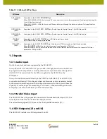
Table 1-1: SW6 and SW7 Settings

Bit Name

Description

TIM861

(

S

W6)

Connected to the G

S

2972 TIM_861 pin. Used to select external CEA-861 timing mode.

When DETECT_TR

S

 is LOW and TIM-861 is LOW, the device extracts all internal timing from the supplied H:V:F 

timing signals. When DETECT_TR

S

 is LOW and TIM-861 is HIGH, the device extracts all internal timing from the 

supplied H

S

YNC, V

S

YNC, DE timing signals.

When DETECT_TR

S

 is HIGH, the device extracts all internal timing from TR

S

 signals em

b

edded in the supplied 

video stream.

S

MPTE_BYPA

SS

n

(

S

W6)

Connected to the G

S

2972 

S

MPTE_BYPA

SS

 pin. Used to ena

b

le/disa

b

le all forms of encoding/decoding, 

scram

b

ling and EDH insertion.

When set LOW, the device operates in Data Through mode (DVB_A

S

I= LOW), or in DVB_A

S

I mode (DVB_A

S

I = 

HIGH). No 

S

MPTE scram

b

ling takes place and none of the I/O processing features of the device are availa

b

le 

when 

S

MPTE_BYPA

SS

 is set LOW.

When set HIGH, the device carries out 

S

MPTE scram

b

ling and I/O processing.

DVB_A

S

I

(

S

W6)

Connected to the G

S

2972 DVB_A

S

I pin. Used to ena

b

le/disa

b

le the DVB-A

S

I data transmission.

When set HIGH, the device will carry out DVB_A

S

I, word-alignment, I/O processing and transmission. The 

S

MPTE_BYPA

SS

 pin must 

b

e set LOW.


When 

S

MPTE_BYPA

SS

 and DVB_A

S

I are 

b

oth set LOW, the device operates in data-through mode.

RATE_

S

EL0, 

RATE_

S

EL1

(

S

W6)

Connected to the G

S

2972 RATE_

S

EL0 and RATE_

S

EL1 pins. Used to configure the operating data rate.

IOPROC_EN/DI

S

n

(

S

W6)

Connected to the G

S

2972 IOPROC_EN/DI

S

 pin. When IOPROC_EN/DI

S

 is HIGH, the I/O processing features of the 

device are ena

b

led. When IOPROC_EN/DI

S

 is LOW, the I/O processing features of the device are disa

b

led. Only 

applica

b

le in 

S

MPTE mode.

20

b

it/10

b

itn

(

S

W6)

Connected to the G

S

2972 20

b

it/10

b

it pin. Used to select the input 

b

us width.

S

DO_EN/DI

S

n

(

S

W6)

Connected to the G

S

2972 

S

DO_EN/DI

S

 pin. Used to ena

b

le or disa

b

le the serial digital output stage.

When 

S

DO_EN/DI

S

 is LOW, the serial digital output signals 

S

DO and 

S

DO are disa

b

led and 

b

ecome 

high-impedance.

When 

S

DO_EN/DI

S

 is HIGH, the serial digital output signals 

S

DO and 

S

DO are ena

b

led.

DETECT_TR

S

(

S

W7)

Connected to the G

S

2972 DETECT_TR

S

 pin. Used to select external HVF timing mode or TR

S

 extraction timing 

mode.

When DETECT_TR

S

 is LOW, the device extracts all internal timing from the supplied H:V:F or CEA-861 timing 

signals, dependent on the status of the TIM861 pin. When DETECT_TR

S

 is HIGH, the device extracts all internal 

timing from TR

S

 signals em

b

edded in the supplied video stream.

RATE_

S

EL0

Data Rate

0

0

1

0

1

X

1.485 or 1.485/1.001G

b

/s

2.97 or 2.97/1.001G

b

/s

270M

b

/s

RATE_

S

EL1

Содержание EB-GS2972

Страница 1: ...EB GS2972 Evaluation Board User Guide 1 of 22 EB GS2972 www gennum com Evaluation Board User Guide 50283 2 May 2012 ...

Страница 2: ...er JP8 8 1 5 2 JTAG Header JP1 8 1 5 3 Lock Status 8 1 6 Modes of Operation 8 2 Board Schematics 9 2 1 Top Level Schematic 9 2 2 Audio Input Schematic 10 2 3 GS2972 Schematic 11 2 4 Power Schematic 12 3 Board Layout 13 4 Bill of Materials 19 Version ECR Date Changes and or Modifications 2 158067 May 2012 Changed R14 value from 380Ω to 200Ω Also changed mistake in 1 5 2 JTAG Header JP1 section 1 15...

Страница 3: ... a parallel video input connector an audio input with four BNCs for AES audio an optional four pin header for serial audio an audio conditioning block a JTAG GSPI header a dip switch and some status indicator LEDs The GS2972 can be configured in SD SDI HD SDI 3G SDI or DVB ASI mode This may be selected manually through a DIP switch The serialized video is available on the SDI output BNC connectors...

Страница 4: ...tion Board User Guide 50283 2 May 2012 4 of 22 Block Diagram of the EB GS2972 GS2972 Transmitter Power SDO SDO 3G SDI 3G SDI 20 bit Video PCLK LED s FVH GSPI 7 GSPI Header Audio DIP Switch AES x4 Serial Audio Group 2 4 ...

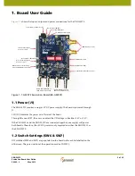
Страница 5: ...her one supply will power both boards Therefore the 5V DC power is only required on either the EB GS2972 or the EB GS2970 1 2 Switch Settings SW6 SW7 DIP switches SW6 and SW7 are populated on the board with each bit labelled on the silk screen They are used to set the operation mode of GS2972 Power Supply Connector J1 DIP Switches SW6 SW7 Audio Input Group One AES 1 J13 AES 2 J14 Audio Input Group...

Страница 6: ...hen set HIGH the device will carry out DVB_ASI word alignment I O processing and transmission The SMPTE_BYPASS pin must be set LOW When SMPTE_BYPASS and DVB_ASI are both set LOW the device operates in data through mode RATE_SEL0 RATE_SEL1 SW6 Connected to the GS2972 RATE_SEL0 and RATE_SEL1 pins Used to configure the operating data rate IOPROC_EN DISn SW6 Connected to the GS2972 IOPROC_EN DIS pin W...

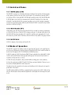
Страница 7: ... pixel clock The related timing signals F V H are on the 10 bit parallel connector J27 1 4 SDI Outputs J3 and J4 The EB GS2972 includes two SDI outputs on J3 and J4 ANC_BLANKn SW7 Connected to the GS2972 ANC_BLANK pin When ANC_BLANK is LOW the Luma and Chroma input data is set to the appropriate blanking levels during the H and V blanking intervals When ANC_BLANK is HIGH the Luma and Chroma data p...

Страница 8: ...populate R114 and R22 However under normal conditions the GS4911B will not need to be programmed 1 5 3 Lock Status LED U25 indicates the lock status of the GS2972 1 6 Modes of Operation The GS2972 supports four distinct modes of operation that can be set through the DIP switch or by programming internal registers through the GSPI These modes are SMPTE mode Data Through mode DVB ASI mode and Standb...

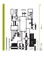
Страница 9: ..._6 GS2972_AES7_8 Audio_RST HVF_IN 2 0 SRC4382_SPI 4 0 PCLK_GS4911 GSPI_GS4911_ 3 0 1 2 3 4 5 6 7 8 9 10 JP8 TSW 105 07 L D Sch_Power Power CS1 GND R107 1 15K PCLK_IN GSPI_GS4911_2 GSPI_GS4911_3 TCK GSPI_GS4911_ 3 0 GSPI_GS4911_0 GSPI_GS4911_1 TMS R114 0R TDI R108 0R SDIN SRC4382_SPI1 GS2972_Audio7 GS2972_Audio6 WCLK_conn GS2972_Audio5 ACLK_conn GS2972_Audio4 GND GND 2 4 6 8 10 12 14 16 18 20 22 24...

Страница 10: ...LRCKB 47 BCKB 48 U27 SRC4382 AES_IN7_8 GND S_AUDIO_0 AES7_8 R93 105R C128 0 1u C127 0 1u VCC_3 3V GND A 3 B 4 R 5 GND 2 Vcc 1 110R U13 SN65LVDT2 GND GND GND SRC4382_SPI1 GND 1V8_SRC4382 S_AUDIO_1 GS2972_AES5_6 AES_IN1_2 S_AUDIO_2 GS2972_AES7_8 AES7_8 AES5_6 R88 1 15K 1V8_SRC4382 S_AUDIO_3 GSPI_GS4911_ 3 0 GS2972_AES5_6 GS4911_genlockb HVF_IN 2 0 SRC4382_SPI1 GS2972_AES5_6 GS2972_AES7_8 GS2972_AES7...

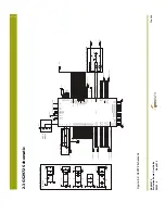
Страница 11: ...ST H8 F DE A3 RATE_SEL1 E4 DIN0 K3 DIN1 J3 U5 GS2972 C40 10n L4 5n6 C19 10n TP9 C14 10n C4 10n C25 1u C3 10n GS2972_PCLK SDOn SDO GS2972_HVF 2 0 GS2972_DIN 19 0 GS2972_RESETn GS2972_Audio 7 0 JTAG 3 0 Pin _ctrl 13 0 GS2972_Locked GNDA_2972 GS2972_GSPI 3 0 GNDA_2972 GNDA_2972 GNDA_2972 VCC_3 3V GNDA_2972 GNDA_2972 VCC_3 3V 1 2V 1 2V CDVDD_2972 1 2VA_2972 IOVDD_2972 3 3VA_2972 1 2VA_2972 1 2VA_2972 ...

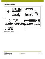
Страница 12: ...K VCC_1 8V C12 22u GND GND VCC_5V IN 5 IN 6 IN 7 IN 8 BIAS 10 PG 9 OUT 1 OUT 18 OUT 19 OUT 20 NC 17 FB 16 EN 11 SS 15 GND 12 NC 13 NC 14 NC 2 NC 3 NC 4 Pad 21 U14 TPS74201_RGW D7 LNJ311G8P GND VCC_5V GND GND GND VCC_3 3V VCC_5V VCC_3 3V VCC_5V GND GND PWRGD_3V3 POWER SUPPLIES C118 10n C117 10n GND IO_V_GS4911 DECOUPLING PINS18 31 38 50 62 R68 0R C96 0 1u C97 0 1u C78 10n C75 10n C76 10n C77 10n C7...

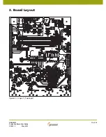
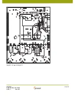
Страница 13: ...EB GS2972 Evaluation Board User Guide 50283 2 May 2012 13 of 22 3 Board Layout Figure 3 1 Layer 1 Top Layer ...

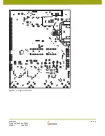
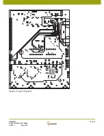
Страница 14: ...EB GS2972 Evaluation Board User Guide 50283 2 May 2012 14 of 22 Figure 3 2 Layer 2 Ground ...

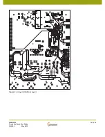
Страница 15: ...EB GS2972 Evaluation Board User Guide 50283 2 May 2012 15 of 22 Figure 3 3 Layer 3 Power ...

Страница 16: ...EB GS2972 Evaluation Board User Guide 50283 2 May 2012 16 of 22 Figure 3 4 Layer 4 Signal 1 ...

Страница 17: ...EB GS2972 Evaluation Board User Guide 50283 2 May 2012 17 of 22 Figure 3 5 Layer 5 Signal 2 ...

Страница 18: ...EB GS2972 Evaluation Board User Guide 50283 2 May 2012 18 of 22 Figure 3 6 Layer 6 Bottom Layer ...

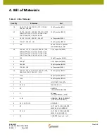
Страница 19: ...C108 C109 C111 C114 C115 C116 C122 C125 C126 C127 C128 C137 C138 C140 C142 C143 C144 C145 C146 C147 C148 0 1μF Capacitor 0603 1 C35 100pF Capacitor 0402 2 C39 C41 4 7μF Capacitor 0603 2 C43 C44 16pF Capacitor 0603 3 C70 C86 C90 1μF Capacitor 0402 15 C74 C75 C76 C77 C78 C82 C83 C88 C98 C99 C100 C101 C102 C117 C118 10nF Capacitor 0402 1 C119 38pF Capacitor 0402 1 C120 24pF Capacitor 0402 1 D7 LNJ311...

Страница 20: ...32 240Ω Resistor 0603 1 R66 49 9kΩ Resistor 0603 2 R72 R73 2Ω Resistor 0805 1 R97 1MΩ Resistor 0402 1 R98 22Ω Resistor 0603 1 R108 0Ω Resistor 0402 2 RN1 RN2 500Ω Resistor Network 1 SW6 SW8_LOGIC_DIP_TH 1 SW7 SW6_LOGIC_DIP_TH 1 S1 B3S 1002 12 TP2 TP3 TP8 TP9 TP10 TP11 TP12 TP16 TP17 TP21 TP22 TP23 Via CT TP 1 U1 MAX6823V SOT23 1 U4 LT3021ES8 1 2 CT SOIC_8 1 U5 GS2972 CT BGA_100_11X11_1 00 4 U10 U1...

Страница 21: ...f 22 2 U24 U28 FXL2TD245 mac010a 1 U25 HSMF C165 2 U26 U27 SRC4382 48 TQFP 1 Y2 CS10 27 000M SM XTAL_6 0X3 5 2 Parts Not To Be Populated 1 R17 DNP 0603 2 R65 R106 DNP 0603 1 R109 DNP 0402 2 R113 R115 DNP 0603 Table 4 1 Bill of Materials Quantity Reference Part ...

Страница 22: ... 6F 4 No 51 Sec 2 Keelung Rd Sinyi District Taipei City 11502 Taiwan R O C Phone 886 2 8732 8879 Fax 886 2 8732 8870 KOREA 8F Jinnex Lakeview Bldg 65 2 Bangidong Songpagu Seoul Korea 138 828 Phone 82 2 414 2991 Fax 82 2 414 2998 DOCUMENT IDENTIFICATION USER GUIDE Information relating to this product and the application or design described herein is believed to be reliable however such information ...

Отзывы: