Cinterion
®
LGA DevKit User Guide
4.3 Pin Headers
27
lga_devkit_ug_v02
2019-05-27
Preliminary
Page 10 of 28
4.3
Pin Headers
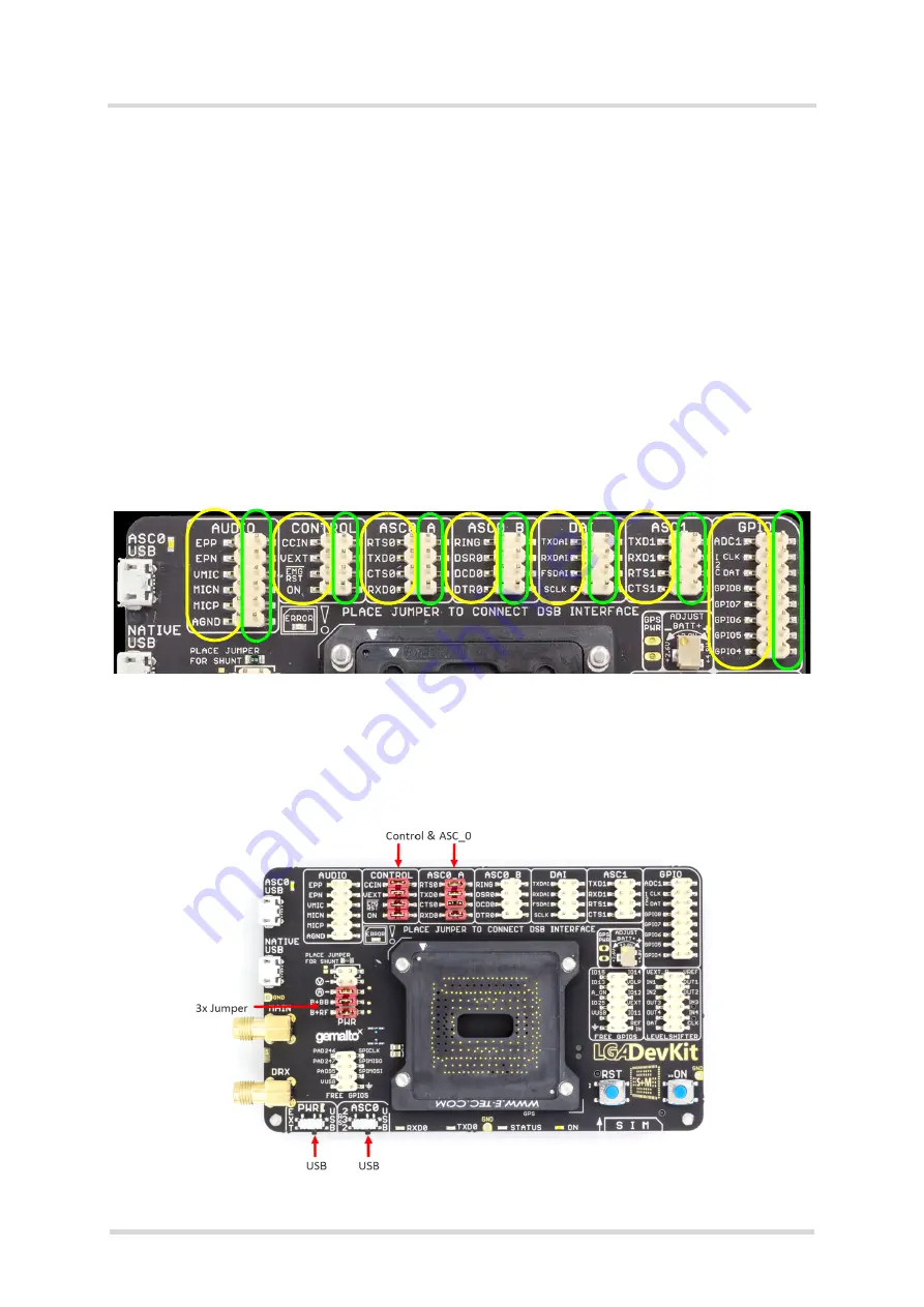
The pin headers at the head of the LGA DevKit's top side can be used to setup connections
between modules and possible on board peripherals. Thus, pin headers having signal names
at their left side only, namely the pin headers AUDIO, CONTROL, ASC0_A, ASC0_B, DAI,
ASC1, GPIO, and PWR, can be bridged by jumpers. All of these pin headers have the module's
signal name on their left side (orange box in Figure 5), whereas the right side corresponds to
peripherals like level shifters or the DSB connector (green box in Figure 5).
•
Placing a jumper connects a line through a level shifter to the associated pin at the 2x40 pin
connector at the bottom of the LGA DevKit (and thus to a connected DSB75/DSB-Mini). See
also
•
Not placing a jumper leaves a module signal line open.
External periphery can also be connected to all accessible module signals directly. When con-
necting other external periphery to the pin headers pay attention not to violate the maximum
module ratings.
Figure 5:
Pin headers
4.3.1
Default Configuration
shows the factory default jumper and switch positioning.
Figure 6:
Figure 6: Default jumper and switch configuration


