GS2011M-DS-001211, Release 0.9
Confidential
Preliminary
19
Chapter 3 GS2011M Architecture
This chapter describes the GainSpan
®
GS2011M Low Power module architecture.
•
Architecture Description, page 19
•
Wireless LAN and System Control Subsystem, page 21
Architecture Description
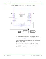
The GainSpan GS2011M module (see
) is based on a highly integrated
GS2000 ultra low power WiFi System-on-Chip (SoC) that contains the following:
•
The GS2000 SoC contains two ARM Cortex M3 CPUs, a compatible 802.11
radio, security, on-chip memory, and variety of peripherals in a single package.
–
One ARM core is dedicated to Networking Subsystems, and the other
dedicated to Wireless LAN Subsystems.
–
The module carries an 802.11/g/n radio with on board 32KHz & 40 MHz
crystal circuitries, RF, and on-board antenna or external antenna options.
•
On module 4 Mega Byte FLASH device that contains the user embedded
applications and data such as web pages.
•
Variety of interfaces are available such as two UART blocks using only two data
lines per port with optional hardware flow controls, two SPI blocks (one SDIO is
shared function with one for the SPI interfaces), I
2
C with Master or slave
operation, JTAG port, low-power 12-bit ADC capable of running at up to 2M
samples/Sec., GPIO’s, and LED Drivers/GPIO with 16mA capabilities.
•
GS2011Mxx has a VRTC pin that is generally connected to always available
power source such as battery or line power. This provides power to the Real Time
Clock (RTC) block on the SoC. The module contains a 1.8V regulator that is
turned on/off when going into the lowest power mode, i.e. standby mode. The
module also has VDDIO power supply input to provide the logic signal level for
the I/O pins. VDDIO must turn on/off with the 1.8V power.


