

1-6-2
E9711DC
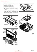
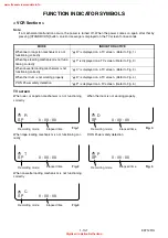
Reference Notes
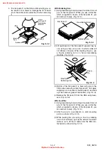
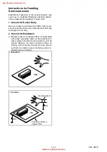
CAUTION 1: Locking Tabs (L-1) and (L-2) are fragile.
Be careful not to break them.
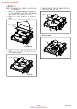
1-1. Release five Locking Tabs (L-1).
1-2. Release three Locking Tabs (L-2)
1-3. Disconnect Connector (CN1505), and remove
the Front Assembly.
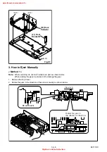
2. When reassembling, solder wire jumpers as shown
in Fig. D8.
3. Before installing the Deck Assembly, be sure to
place the pin of LD-SW on Main CBA as shown in
Fig. D8. Then, install the Deck Assembly while
aligning the hole of Cam Gear with the pin of LD-
SW, the shaft of Cam Gear with the hole of LD-SW
as shown in Fig. D8.
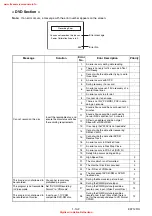
(S-1)
(S-1)
(S-1)
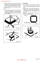
[1] Top Cover
Fig. D1
(L-1)
(S-2)
(S-2)
(S-3)
(L-2)
(L-1)
(L-1)
[2] Front
Assembly
[3] Front
Bracket
[4] Radiation Sheet
CN1505
Fig. D2
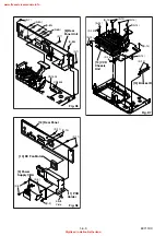
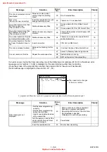
Fig. D3
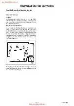
(S-4)
Jack Earth Plate
[5] Jack Bracket
[6] Front
Jack CBA
Fig. D4
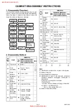
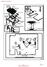
(S-5B)
(S-5A)
(S-5A)
[7] DVD
Mechanism
&
DVD Main
CBA
Assembly
CN501
CN601
www.freeservicemanuals.info
Digitized in Heiloo Netherland


