


1-4-1
DVD_NOTE
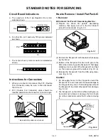
STANDARD NOTES FOR SERVICING
Circuit Board Indications
a. The output pin of the 3 pin Regulator ICs is indi-
cated as shown.
b. For other ICs, pin 1 and every fifth pin are indicated
as shown.
c. The 1st pin of every male connector is indicated as
shown.
Instructions for Connectors
1. When you connect or disconnect the FFC (Flexible
Foil Connector) cable, be sure to first disconnect
the AC cord.
2. FFC (Flexible Foil Connector) cable should be
inserted parallel into the connector, not at an angle.
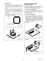
How to Remove / Install Flat Pack-IC
1. Removal
With Hot-Air Flat Pack-IC Desoldering Machine:.
(1) Prepare the hot-air flat pack-IC desoldering
machine, then apply hot air to the Flat Pack-IC
(about 5 to 6 seconds). (Fig. S-1-1)
(2) Remove the flat pack-IC with tweezers while apply-
ing the hot air.
(3) Bottom of the flat pack-IC is fixed with glue to the
CBA; when removing entire flat pack-IC, first apply
soldering iron to center of the flat pack-IC and heat
up. Then remove (glue will be melted). (Fig. S-1-6)
(4) Release the flat pack-IC from the CBA using twee-
zers. (Fig. S-1-6)
Caution:
1. Do not supply hot air to the chip parts around the
flat pack-IC for over 6 seconds because damage to
the chip parts may occur. Put masking tape around
the flat pack-IC to protect other parts from damage.
(Fig. S-1-2)
2. The flat pack-IC on the CBA is affixed with glue, so
be careful not to break or damage the foil of each
pin or the solder lands under the IC when removing
it.
Top View
Out
In
Bottom View
Input
5
10
Pin 1
Pin 1
FFC Cable
Connector
CBA
* Be careful to avoid a short circuit.
Fig. S-1-1
Hot-air
Flat Pack-IC
Desoldering
Machine
CBA
Flat Pack-IC
Tweezers
Masking
Tape
Fig. S-1-2
Содержание DPVR-4604
Страница 29: ...Main 1 10 Schematic Diagram VCR Section 1 10 3 1 10 4 H95B0SCM1...
Страница 31: ...1 10 7 1 10 8 H95B0SCM3 Main 3 10 Schematic Diagram VCR Section...
Страница 32: ...Main 4 10 Schematic Diagram VCR Section 1 10 9 1 10 10 H95B0SCM4...
Страница 33: ...Main 5 10 Schematic Diagram VCR Section 1 10 11 1 10 12 H95B0SCM5...
Страница 34: ...Main 6 10 Schematic Diagram VCR Section 1 10 13 1 10 14 H95B0SCM6...
Страница 35: ...Main 7 10 Schematic Diagram VCR Section 1 10 15 1 10 16 H95B0SCM7...
Страница 36: ...Main 8 10 DVD Open Close Schematic Diagram VCR Section 1 10 17 1 10 18 H95B0SCM8...
Страница 37: ...1 10 19 1 10 20 Main 9 10 Schematic Diagram VCR Section H95B0SCM9...
Страница 38: ...Main 10 10 Schematic Diagram VCR Section 1 10 21 1 10 22 H95B0SCM10...
Страница 40: ...1 10 25 1 10 26 Jack Schematic Diagram VCR Section H95B0SCJ...
Страница 41: ...1 10 27 1 10 28 Function Schematic Diagram VCR Section H95B0SCF...
Страница 42: ...1 10 29 1 10 30 AFV Schematic Diagram VCR Section H95B0SCAFV...
Страница 44: ...1 10 33 Main CBA Bottom View BH9510F01014A 1 10 34...
Страница 48: ...DVD Main 1 3 Schematic Diagram DVD Section H95B0SCD1 1 10 41 1 10 42...
Страница 49: ...1 10 43 1 10 44 DVD Main 2 3 Schematic Diagram DVD Section H95B0SCD2...
Страница 51: ...DVD Main 3 3 Schematic Diagram DVD Section 1 10 47 H95B0SCD3 1 10 48...
Страница 78: ...3 1 3 H95B0PEX S1 A14 X20 Some Ref Numbers are not in sequence X2 X3 X4 X1 Unit S3 S2 S2 X5 S7 Packing...
Страница 98: ...DPVR 4604 H95B0ED...