


1-6-2
H95B0DC
Reference Notes
CAUTION 1: Locking Tabs (L-1) are fragile. Be careful
not to break them.
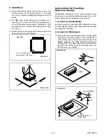
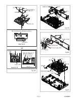
1-1. Remove Screw (S-3).
1-2. Release seven Locking Tabs (L-1) (to do this, first
release five Locking Tabs (A) at the side and top,
and then release two Locking Tabs (B) at the bot-
tom.)
CAUTION 2: Electrostatic breakdown of the laser
diode in the optical system block may occur as a
potential difference caused by electrostatic charge
accumulated on cloth, human body etc., during
unpacking or repair work.
To avoid damage of pickup follow next procedures.
2-1. Slide the pickup unit as shown in Fig. D4.
2-2. Short the three short lands of FPC cable with sol-
der before removing the FFC cable (CN301) from
it. If you disconnect the FFC cable (CN301), the
laser diode of pickup will be destroyed. (Fig. D4)
2-3. Disconnect Connector (CN201). Remove two
Screws (S-5) and lift the DVD Main CBA. (Fig.
D4)
CAUTION 3: When reassembling, confirm the FFC
cable (CN301) is connected completely. Then remove
the solder from the three short lands of FPC cable.
(Fig. D4)
CAUTION 4: When reassembling, solder wire jumpers
as shown in Fig. D8.
CAUTION 5: Before installing the Deck Assembly, be
sure to place the pin of LD-SW on Main CBA as shown
in Fig. D8. Then, install the Deck Assembly while
aligning the hole of Cam Gear with the pin of LD-SW,
the shaft of Cam Gear with the hole of LD-SW as
shown in Fig. D8.
(S-1)
[1] Top Cover
(S-1)
(S-1)
Fig. D1
(S-3)
(S-3A)
(S-3A)
[3] Top Bracket
(L-1)
(L-1)
(L-1)
[2] Front Assembly
(B)
(A)
(A)
(A)
(S-2)
Fig. D2
(S-4)
(S-4)
CN601
CN401
(S-4)
[4] DVD Mecha Assembly
CN302
Fig. D3
Содержание DPVR-4604
Страница 29: ...Main 1 10 Schematic Diagram VCR Section 1 10 3 1 10 4 H95B0SCM1...
Страница 31: ...1 10 7 1 10 8 H95B0SCM3 Main 3 10 Schematic Diagram VCR Section...
Страница 32: ...Main 4 10 Schematic Diagram VCR Section 1 10 9 1 10 10 H95B0SCM4...
Страница 33: ...Main 5 10 Schematic Diagram VCR Section 1 10 11 1 10 12 H95B0SCM5...
Страница 34: ...Main 6 10 Schematic Diagram VCR Section 1 10 13 1 10 14 H95B0SCM6...
Страница 35: ...Main 7 10 Schematic Diagram VCR Section 1 10 15 1 10 16 H95B0SCM7...
Страница 36: ...Main 8 10 DVD Open Close Schematic Diagram VCR Section 1 10 17 1 10 18 H95B0SCM8...
Страница 37: ...1 10 19 1 10 20 Main 9 10 Schematic Diagram VCR Section H95B0SCM9...
Страница 38: ...Main 10 10 Schematic Diagram VCR Section 1 10 21 1 10 22 H95B0SCM10...
Страница 40: ...1 10 25 1 10 26 Jack Schematic Diagram VCR Section H95B0SCJ...
Страница 41: ...1 10 27 1 10 28 Function Schematic Diagram VCR Section H95B0SCF...
Страница 42: ...1 10 29 1 10 30 AFV Schematic Diagram VCR Section H95B0SCAFV...
Страница 44: ...1 10 33 Main CBA Bottom View BH9510F01014A 1 10 34...
Страница 48: ...DVD Main 1 3 Schematic Diagram DVD Section H95B0SCD1 1 10 41 1 10 42...
Страница 49: ...1 10 43 1 10 44 DVD Main 2 3 Schematic Diagram DVD Section H95B0SCD2...
Страница 51: ...DVD Main 3 3 Schematic Diagram DVD Section 1 10 47 H95B0SCD3 1 10 48...
Страница 78: ...3 1 3 H95B0PEX S1 A14 X20 Some Ref Numbers are not in sequence X2 X3 X4 X1 Unit S3 S2 S2 X5 S7 Packing...
Страница 98: ...DPVR 4604 H95B0ED...