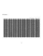
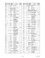
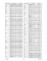
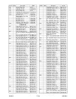
background image

WAVEFORMS

WF3

WF2

WF3

UPPER

WF1

WF1

LOWER

TP751

TP751

TP504

UPPER

LOWER

TP504

TP301

WF4

WF6

Pin 6 of IC1403

WF5

VIDEO-C

WF7

AUDIO-L

1V

0.5ms

WF8 

WF9

SPDIF

1V

0.1

µ

s           

Pin 8 of CN1601

Pin 10 of CN1601

Pin 13 of CN1601

Pin 15 of CN1601

Pin 18 of CN1601

NOTE:

Input
   VCR: COLOR BAR SIGNAL (WITH 1KHz AUDIO SIGNAL)
            (WF1~WF3)
   DVD: POWER ON (STOP) MODE
            (WF4~WF6)  
     CD: 1kHz PLAY
            (WF7~WF9)

AUDIO-R

1V

0.5ms

V-OUT E-E

0.2V

20

µ

s

V-OUT 

0.5V

50

µ

s

RF-SW

5V

C-PB 
RF-SW

5V

5ms

0.2V

VIDEO-Y

0.2V

20

µ

s

VIDEO-C

0.2V

20

µ

s

VIDEO-CVBS

0.5V

20

µ

s

1-13-1

H9903WF

Содержание DDVR-6830

Страница 1: ...0 DPVR 6830 Main Section I Specifications I Preparation for Servicing I Adjustment Procedures I Schematic Diagrams I CBA s I Exploded views I Parts List When servicing the deck mechanism refer to MK14...

Страница 2: ...1 Function Indicator Symbols 1 10 1 Block Diagrams 1 11 1 Schematic Diagrams CBA s and Test Points 1 12 1 Waveforms 1 13 1 Wiring Diagram VCR Section 1 14 1 Wiring Diagram DVD Section 1 14 2 IC Pin Fu...

Страница 3: ...de W O Burst 1 4 Video Color S N AM R P dB 37 41 SP Mode 1 5 Video Color S N PM R P dB 30 36 SP Mode 1 6 Resolution PB Line 230 245 SP Mode 2 Servo 2 1 Jitter Low sec 0 07 0 12 SP Mode 2 2 Wow Flutter...

Страница 4: ...re 5 C 40 C ITEM CONDITIONS UNIT NOMINAL LIMIT 1 Video Output 75 load Vpp 1 0 0 1 2 Optical Digital Out dBm 18 3 Audio PCM 3 1 Output Level 1 kHz 0 dB 47k load Vrms 2 0 3 2 S N 47k load dB 90 3 3 Freq...

Страница 5: ...is turned on Do not look directly at the laser beam CAUTION Use of controls and adjustments or doing procedures other than those specified herein may result in hazardous radiation exposure Location T...

Страница 6: ...especially 1 Wires covered with PVC tubing 2 Double insulated wires 3 High voltage leads D Use specified insulating materials for hazardous live parts Note especially 1 Insulation tape 2 PVC tubing 3...

Страница 7: ...age Current Test Confirm the specified or lower leakage current between B earth ground power cord plug prongs and externally exposed accessible parts RF termi nals antenna terminals video and audio in...

Страница 8: ...achine then apply hot air to the Flat Pack IC about 5 to 6 seconds Fig S 1 1 2 Remove the flat pack IC with tweezers while apply ing the hot air 3 Bottom of the flat pack IC is fixed with glue to the...

Страница 9: ...removing entire flat pack IC first apply soldering iron to center of the flat pack IC and heat up Then remove glue will be melted Fig S 1 6 4 Release the flat pack IC from the CBA using twee zers Fig...

Страница 10: ...Installation 1 Using desoldering braid remove the solder from the foil of each pin of the flat pack IC on the CBA so you can install a replacement flat pack IC more easily 2 The I mark on the flat pac...

Страница 11: ...ed to remove any static electricity that may be charged on the body 2 Ground for Workbench 1 Be sure to place a conductive sheet or copper plate with proper grounding 1M on the workbench or other surf...

Страница 12: ...nto the Deck Mechanism Assembly and press the PLAY button The tape will be loaded into the Deck Mechanism Assembly Make sure the power is on connect TP501 S INH to GND This will stop the function of T...

Страница 13: ...ference Notes ID LOC No PART REMOVAL Fig No REMOVE UNHOOK UNLOCK RELEASE UNPLUG DESOLDER Note 1 Top Case D1 8 S 1 2 Front Assembly D2 3 L 1 3 L 2 1 1 1 1 2 3 Top Bracket D2 3 S 2 4 DVD Mechanism Assem...

Страница 14: ...ig D4 2 2 Short the three short lands of FPC cable with sol der before removing the FFC cable CN201 from it If you disconnect the FFC cable CN201 the laser diode of pickup will be destroyed Fig D4 CAU...

Страница 15: ...te 6 Power Supply CBA 7 Loader Holder 4 DVD Mechanism Assembly Fig D3 CN201 CN301 S 7 8 DVD Main CBA Unit DVD Mechanism A Fig D4 S 7 View for A Short the three short lands by soldering Either of two p...

Страница 16: ...y Fig D6 Desolder Lead with blue stripe From FE Head BOTTOM VIEW Lead connections of Deck Assembly and Main CBA Desolder From Capstan Motor Assembly Printing side Desolder From Cylinder Assembly From...

Страница 17: ...Mechanism HOW TO EJECT MANUALLY 1 Remove the Top Case Front Assembly and Top Bracket 2 Remove four Screws S 3 in Fig D3 Do not disconnect connectors 3 While lifting up the DVD Mechanism rotate the rou...

Страница 18: ...Dual trace with 10 1 probe V Range 0 001 50V Div F Range DC AC 20MHz 2 Alignment Tape FL6A Head Switching Position Adjustment Purpose To determine the Head Switching position during playback Symptom o...

Страница 19: ...unit in that order Fig a appears on the screen 2 Press CLEAR C RESET button on the remote control unit Fig b appears on the screen When OK appears on the screen the factory default will be set 3 To e...

Страница 20: ...e appears on the VFD Fig f At this time no button is available 6 Remove the disc on the tray 7 Unplug the AC cord from the AC outlet Then plug it again 8 Turn the power on by pressing the STANDBY ON...

Страница 21: ...appears on the screen When OK appears on the screen the factory default will be set Then the firmware renewal mode is complete 11 To exit this mode press STANDBY ON button MODEL Version Region EEPROM...

Страница 22: ...ctly When the drum is not working properly P ON Power safety detection MODE INDICATOR ACTIVE When reel or capstan mechanism is not functioning correctly A R is displayed on a TV screen Refer to Fig 1...

Страница 23: ...POWER C SYNC INPUT SELECT DVD POWER C SYNC OUTPUT SELECT IIC BUS SCL LD SW 9 AL 5V AL 5V SW507 LD SW AL 5V D555 S LED TO POWER SUPPLY BLOCK DIAGRAM TP501 SENS INH IC501 SERVO SYSTEM CONTROL LINE MUTE...

Страница 24: ...94 93 90 89 88 87 CHARA INS CCD 1H DELAY SP BYPASS MUTE PB EE IN1 TUNER IN1 TUNER MUTE PB EE FRT IN2 FRT IN2 AGC P R R Y C P R P R P EP Y DELAY Y C MIX 21 79 78 AGC VXO OSD CHARACTER MIX FBC 1 2 58 5...

Страница 25: ...TROL MUTE 11 6 PB ON SP LP ON P TUNER IN2 IN1 R ALC DET ALC IC301 AUDIO SIGNAL PROCESS 15 13 17 4 AUDIO PB REC CN504 3 A COM 1 AE H 2 AE H FE H AUDIO HEAD AUDIO ERASE HEAD ACE HEAD ASSEMBLY FE HEAD 2...

Страница 26: ...AMP REC AUDIO SIGNAL PB AUDIO SIGNAL Mode SP REC DVD AUDIO SIGNAL AFV CBA JK101 2 6 2 6 1 3 1 3 JK1402 TU AUDIO R 4 TU AUDIO L 5 4 5 CN701 CN1 CN701 CN1 TU701 TUNER UNIT SIF OUT 22 ALC SW SW ALC 67 65...

Страница 27: ...5V 7 CL052A CL052B 1 AL 30V 3 AL 2 8V 5 AL 4V 8 F1 7 1 3 5 8 7 F2 TO PIN 67 OF IC501 TO PIN 32 OF IC501 TO PIN 66 OF IC501 IC1003 3 3V REG IC1002 1 2V REG JUNCTION CBA CN051A 1 3 5 7 1 3 5 7 9 11 13...

Страница 28: ...FP CLK CN401 DVD MAIN CBA UNIT DRIVE CBA IC301 SERVO DRIVE CN301 M SLED MOTOR M SPINDLE MOTOR MICRO CONTROLLER SLED MOTOR DRIVE FOCUS ACTUATOR DRIVE SPINDLE MOTOR DRIVE TRACKING ACTUATOR DRIVE 147 TRA...

Страница 29: ...MER DECODER I F CPU I F READ MEMORY DATA RAM DSP DECODER I O PROCESSOR INST ROM DATA RAM INST ROM SERIAL D A GENERAL I O INTERRUPT CONTROLLER TIMER WATCH DOG TIMER REMOTE CONTROL 32BIT CPU STREAM I F...

Страница 30: ...SIGNAL 18 18 SPDIF AUDIO MUTE Q1204 W F 9 5 W F 7 W F 8 CN601 1 1 VIDEO Y I 10 10 VIDEO C 4 4 VIDEO Pr Cr 8 8 VIDEO Y I P 6 6 VIDEO Pb Cb VIDEO Y I VIDEO C VIDEO Pr Cr VIDEO Y I P 3 3 ASPECT FROM DIGI...

Страница 31: ...itute replacement parts that do not have the same safety characteristics as specified in the parts list may create shock fire or other hazards Notes 1 Do not use the part number shown on these draw in...

Страница 32: ...acement parts which are listed with their part numbers in the parts list section of the service manual 4 Voltage indications for PLAY and REC modes on the schematics are as shown below 5 How to read c...

Страница 33: ...1 12 3 H9903SCM1 Main 1 8 Schematic Diagram VCR Section Comparison Chart of Models and Marks MODEL MARK DDVR 6830 A DPVR 6830 B...

Страница 34: ...e f g c d e f g h i i a b a b a b a b a b IC611 MATRIX CHART REPEAT TITLE GROUP VCR CHP REC SACD TRK ALL B PSCAN DVD P M HD V CD A A 5G 4G 3G 2G 1G 7G 6G a d g c b e f f i i REPEAT TITLE GROUP VCR CHP...

Страница 35: ...1 12 5 H9903SCM3 Main 3 8 Schematic Diagram VCR Section Comparison Chart of Models and Marks MODEL MARK DDVR 6830 A DPVR 6830 B...

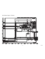
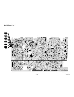
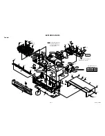
Страница 36: ...1 12 6 H9903SCM4 Main 4 8 Schematic Diagram VCR Section...

Страница 37: ...1 12 7 H9903SCM5 Main 5 8 Schematic Diagram VCR Section...

Страница 38: ...1 12 8 H9903SCM6 Main 6 8 Schematic Diagram VCR Section...

Страница 39: ...1 12 9 H9903SCM7 Main 7 8 DVD Open Close Schematic Diagram VCR Section Comparison Chart of Models and Marks MODEL MARK DDVR 6830 A DPVR 6830 B...

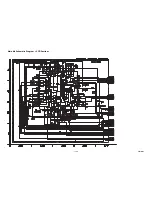
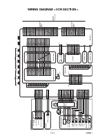
Страница 40: ...1 12 10 H9903CM8 Main 8 8 Schematic Diagram VCR Section...

Страница 41: ...check to see that all components in the power supply circuit are not defective before you connect the AC plug to the AC power supply Otherwise it may cause some components in the power supply circuit...

Страница 42: ...1 12 12 H9903SCJ Jack A Schematic Diagram VCR Section...

Страница 43: ...1 12 13 H9903SCAFV AFV Schematic Diagram VCR Section...

Страница 44: ...1 12 14 DVD Main 1 3 Schematic Diagram DVD Section 1 NOTE Either IC461 or IC462 is used for DVD MAIN CBA UNIT H9903SCD1...

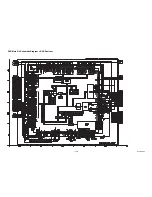
Страница 45: ...1 12 15 H9903SCD2 DVD Main 2 3 Schematic Diagram DVD Section...

Страница 46: ...3 2 3 32 64 0 0 96 128 1 7 1 7 PIN NO PLAY STOP PIN NO PLAY STOP PIN NO PLAY STOP PIN NO PLAY STOP 129 2 3 2 3 161 3 4 3 4 193 225 3 4 3 4 130 2 3 2 3 162 0 0 194 226 131 2 3 2 3 163 1 8 1 8 195 227...

Страница 47: ...1 12 17 H9903SCD3 DVD Main 3 3 Schematic Diagram DVD Section...

Страница 48: ...1 12 18 Main CBA Top View SW P VR501 CTL TP503 RF SW TP504 WF1 S INH TP501 V OUT TP751 WF3 C PB TP301 WF2 BHF300F01011A BHF300F01011B Sensor CBA Top View BH9900F01013A...

Страница 49: ...1 12 19 PIN13OF CN1601 WF5 PIN 10 OF CN1601 WF4 PIN 8 OF CN1601 WF8 PIN 15 OF CN1601 WF6 PIN 6 OF IC1403 WF9 PIN 18 OF CN1601 WF7 Main CBA Bottom View BH9900F01013A...

Страница 50: ...1 12 20 BH9900F01013C DVD Open Close CBA Top View DVD Open Close CBA Bottom View Jack A CBA Top View Jack A CBA Bottom View BH9900F01022C AFV CBA Top View AFV CBA Bottom View BE6800F01091...

Страница 51: ...selectable power supply circuit is used in this unit If Main Fuse F1001 is blown check to see that all components in the power supply circuit are not defective before you connect the AC plug to the A...

Страница 52: ...1 s Pin 8 of CN1601 Pin 10 of CN1601 Pin 13 of CN1601 Pin 15 of CN1601 Pin 18 of CN1601 NOTE Input VCR COLOR BAR SIGNAL WITH 1KHz AUDIO SIGNAL WF1 WF3 DVD POWER ON STOP MODE WF4 WF6 CD 1kHz PLAY WF7 W...

Страница 53: ...EV 1 2V EV 1 2V EV 3 3V EV 3 3V EV 3 3V DVD P ON 3 3V DVD P ON 5V EV 11V EV 11V GND GND GND GND GND GND GND PWRCON FP CLK FP DIN FP STB REMOTE DVD FP DOUT NU 23 24 25 26 DVD POWER DVD OPEN CLOSE DVD...

Страница 54: ...AUDIO 5V DVD AUDIO R AUDIO 5V SPDIF 13 14 15 16 17 18 CN401 CN601 PICK UP UNIT CN201 1 2 3 4 5 6 7 8 9 10 11 12 13 14 15 16 17 18 19 20 TS TS FS CD LD FS GND DVD PD GND CD PD PD MONI DVD LD VREF E GN...

Страница 55: ...Head Amp Switching Pulse H L 17 IN H A COMP Head Amp Comparator Signal H L 18 OUT RF SW Video Head Switching Pulse H L 19 OUT Hi Fi H SW HiFi Audio Head Switching Pulse H L 20 NU Not Used 21 OUT DVD...

Страница 56: ...Control Clock H L Pin No Mark IN OUT Signal Name Function Active Level 72 IN OUT IIC BUS SDA IIC BUS Control Data H L 73 NU Not Used 74 NU Not Used 75 IN DVD POWER MONITOR DVD Power Monitor Signal P...

Страница 57: ...nal Name Name Function 1 IN FP CLK Clock Input 2 IN FP STB Serial Interface Strobe 3 NU Not Used 4 NU Not Used 5 VSS GND 6 VDD Power Supply 7 OUT a Segment Output 8 b 9 c 10 d 11 e 12 f 13 g 14 h 15 V...

Страница 58: ...4053BF N 1 MID 32A22F PT204 6B 12 E C 35 7 BT 298NYM 1 5 4 8 1 BR24L02F WE2 CAT24WC02WI TE13 28 15 14 PT6313 S TP L SC16313G 1 0C 0805T 002 JST1162 GP1FA513TZ0F 1 2 3 B1 E B2 C1 C2 FMG4A T148 RN1511 T...

Страница 59: ...W007 JW002 JW001 2L091 2L012 2L054 2B55 B AFV CBA Main CBA Jack A CBA Power Supply CBA Junction CBA 2L021 F1001 A B A A3 A7 A21 A 2B5 2L012 2L041 2L041 2L041 2L041 2L041 2L041 A2 2L041 2L041 2B18 2B16...

Страница 60: ...2 H9903PEX Packing S1 A14 X4 Unit S3 S2 S2 S2 S2 X5 S7 Some Ref Numbers are not in sequence X20E A X20F X20D X20C X20B X20A X2 X3 X1 Comparison Chart of Models and Marks Model Mark DDVR 6830 DPVR 6830...

Страница 61: ...2B54 PLATE GROUND RCA H9700ED 0VM306867 2B55 PLATE GROUND 21P H9700ED 0VM416444 2L011 P TIGHT SCREW 3X8 BIND GBMP3080 2L012 SCREW S TIGHT M3X6 BIND HEAD GBMS3060 2L020 P TIGHT SCREW 3X8 BIND GBMP3080...

Страница 62: ...50V CHD1JK30B102 C116 CHIP CERAMIC CAP B K 2200pF 50V CHD1JK30B222 C117 ELECTROLYTIC CAP 1 F 50V M or CE1JMASDL1R0 ELECTROLYTIC CAP 1 F 50V M CE1JMASTL1R0 C118 CHIP CERAMIC CAP B K 2200pF 50V CHD1JK3...

Страница 63: ...MIC CAP CH J 120pF 50V or CHD1JJ3CH121 Ref No Mark Description Part No CHIP CERAMIC CAP CG J 120pF 50V CHD1JJ3CG121 C340 ELECTROLYTIC CAP 1 F 50V M H7 CE1JMAVSL1R0 C341 CHIP CERAMIC CAP 1608 CH D 10pF...

Страница 64: ...5V or CHD1EZ30F104 CHIP CERAMIC CAP FZ Z 0 1 F 50V CHD1JZ3FZ104 C502 CHIP CERAMIC CAP 1608 B K 0 022 F 50V or CHD1JK30B223 Ref No Mark Description Part No CHIP CERAMIC CAP 1608 B K 0 022 F 25V CHD1EK3...

Страница 65: ...3V M CE0KMASTL101 C1042 ELECTROLYTIC CAP 470 F 6 3V M or CE0KMASDL471 ELECTROLYTIC CAP 470 F 6 3V M CE0KMASTL471 Ref No Mark Description Part No C1050 CHIP CERAMIC CAP 1608 B K 0 33 F 10V CHD1AK30B33...

Страница 66: ...33 T 77 QDTZ001SS133 D511 ZENER DIODE DZ 7 5BSAT265 or NDTA0DZ7R5BS ZENER DIODE MTZJT 777 5A QDTA0MTZJ7R5 D512 SWITCHING DIODE 1N4148M or NDTZ01N4148M SWITCHING DIODE 1SS133 T 77 QDTZ001SS133 Ref No M...

Страница 67: ...Y AT P or NQSYKTC3199P TRANSISTOR KTC3199 GR AT P or NQS4KTC3199P Ref No Mark Description Part No TRANSISTOR 2SC1815 Y TE2 F T or QQSY2SC1815F TRANSISTOR 2SC1815 GR TE2 F T or QQS12SC1815F TRANSISTOR...

Страница 68: ...S12SC1815F TRANSISTOR 2SC2785 J or QQSJ02SC2785 TRANSISTOR 2SC2785 H or QQSH02SC2785 TRANSISTOR 2SC2785 F or QQSF02SC2785 Ref No Mark Description Part No TRANSISTOR KTC3199 Y or NQSY0KTC3199 TRANSISTO...

Страница 69: ...5 6k RRXAJR5Z0562 R461 CHIP RES 1608 1 10W J 47k RRXAJR5Z0473 R462 CHIP RES 1608 1 10W J 10k RRXAJR5Z0103 Ref No Mark Description Part No R463 CHIP RES 1608 1 10W J 470 RRXAJR5Z0471 R464 CHIP RES 1608...

Страница 70: ...BON RES 1 4W J 1k RCX4JATZ0102 R1062 CHIP RES 1608 1 10W J 10k RRXAJR5Z0103 Ref No Mark Description Part No R1065 CHIP RES 1608 1 10W J 10k RRXAJR5Z0103 R1066 CHIP RES 1608 1 10W J 220k RRXAJR5Z0224 R...

Страница 71: ...UTUNPLGAL015 VR501 CARBON P O T VZ067TL1 B104 PB F VRCB104HH014 X301 XTAL 4 433619MHz or FXC445LLN004 XTAL 1K 044334EE or FXC445LDS002 QUARTZ CRYSTAL 4 433619MHz or FXC445LCHE01 XTAL 4 433619MHz or F...

Страница 72: ...EL817A or NPEA000EL817 PHOTOCOUPLER EL817B or NPEB000EL817 PHOTOCOUPLER PS2561A 1 Q or QPEQPS2561A1 PHOTOCOUPLER PS2561A 1 W QPEWPS2561A1 COILS L010 CHOKE COIL 47 H or LLBD00PKV022 Ref No Mark Descrip...

Страница 73: ...ABLE 8P AWG26 2651 P2 0 75 WX3808S6FF07 JW002 FLAT CABLE 9P AWG26 2651 P2 0 65 WX3809S6FF06 Ref No Mark Description Part No Ref No Mark Description Part No JACK A CBA PSV C Consists of the following C...

Страница 74: ...Z104 C20 ELECTROLYTIC CAP 3 3 F 50V M H7 CE1JMASSL3R3 C21 CHIP CERAMIC CAP 1608 F Z 0 1 F 50V or CHD1JZ30F104 CHIP CERAMIC CAP 1608 F Z 0 1 F 25V or CHD1EZ30F104 CHIP CERAMIC CAP FZ Z 0 1 F 50V CHD1JZ...

Страница 75: ...DDVR 6830 DPVR 6830 H9903 04ED 2005 07 23...

Отзывы: