


171
CHAPTER 7 DETAILED EXECUTION INSTRUCTIONS
7.75
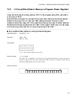
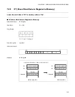
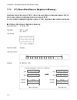
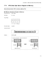
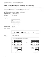
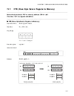
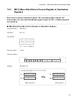
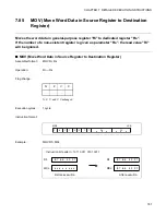
ST (Store Word Data in Program Status Register to Memory)
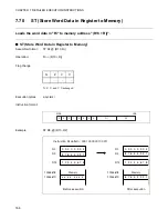
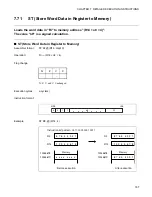
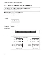
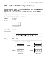
Subtracts 4 from the value of "R15", stores the word data in the program status (PS) to
the memory address indicated by the new value of "R15".
■
ST (Store Word Data in Program Status Register to Memory)
Assembler format:
ST PS, @ – R15
Operation:
R15 – 4
→
R15
PS
→
(R15)
Flag change:
N, Z, V, and C: Unchanged
Execution cycles:
a cycle(s)
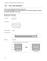
Instruction format:
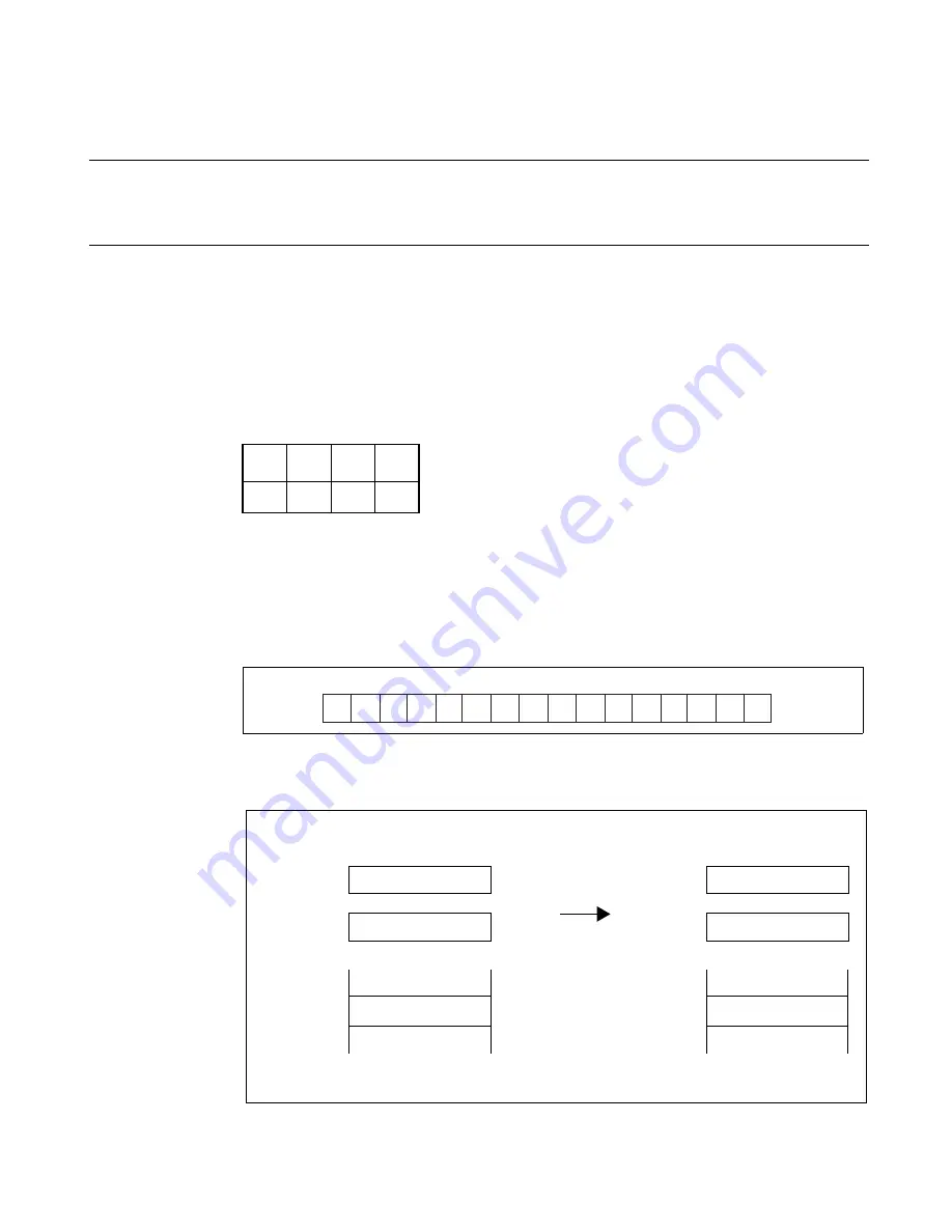
Example:
ST PS, @ – R15
N
Z
V
C
–
–
–
–
MSB
LSB
0
0
0
1
0
1
1
1
1
0
0
1
0
0
0
0
12
3
45670
R15
R15
F F F
8
F
8
C 0
F F F
8
F
8
C 0
12
3
45670
12
3
45674
12
3
45674
1 2
3
4
5 6 7
8
F F F
8
F
8
C 0
P
S
1 2
3
4
5 6 7 4
P
S
x x x x
x x x x
Memory
Memory
Before exec
u
tion
After exec
u
tion
In
s
tr
u
ction
b
it p
a
ttern : 0001 0111 1001 0000
Содержание FR Family
Страница 2: ......
Страница 3: ...FUJITSU LIMITED FR Family 32 BIT MICROCONTROLLER INSTRUCTION MANUAL ...
Страница 4: ......
Страница 8: ...iv ...
Страница 14: ...x ...
Страница 36: ...12 CHAPTER 2 MEMORY ARCHITECTURE ...
Страница 284: ...260 CHAPTER 7 DETAILED EXECUTION INSTRUCTIONS ...
Страница 301: ...277 INDEX INDEX The index follows on the next page This is listed in alphabetical order ...
Страница 314: ......