


Pulse-Width Modulation (PWM) Module
MCF52110 ColdFire® Integrated Microcontroller Reference Manual, Rev. 1
Freescale Semiconductor
26-11
Preliminary
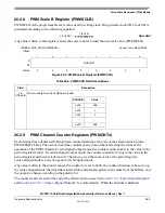
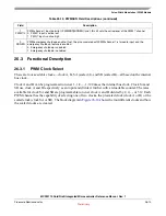
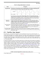
26.2.11 PWM Channel Duty Registers (PWMDTY
n
)
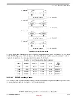
The PWM duty registers determine the duty cycle of the associated PWM channel. To calculate the output
duty cycle (high time as a percentage of period) for a particular channel:
Eqn. 26-4
For boundary case programming values (e.g. PWMDTY
n
= 0x00 or PWMDTY
n
> PWMPER
n
), refer to
Section 26.3.2.8, “PWM Boundary Cases”
.
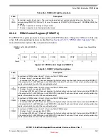
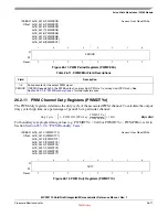
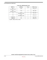
IPSBAR
Offset:
0x1B_0014 (PWMPER0)
0x1B_0015 (PWMPER1)
0x1B_0016 (PWMPER2)
0x1B_0017 (PWMPER3)
0x1B_0018 (PWMPER4)
0x1B_0019 (PWMPER5)
0x1B_001A (PWMPER6)
0x1B_001B (PWMPER7)
Access: User Read/Write
7
6
5
4
3
2
1
0
R
PERIOD
W
Reset:
1
1
1
1
1
1
1
1
Figure 26-11. PWM Period Registers (PWMPER
n
)
Table 26-11. PWMPER
n
Field Descriptions
Field
Description
7–0
PERIOD
Period counter for the output PWM signal.
If PERIOD equals 0x00, the PWM
n
output is always high (PPOL
n
=1) or always low (PPOL
n
=0). See
Section 26.3.2.8, “PWM Boundary Cases”
for other special cases.
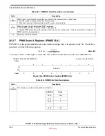
IPSBAR
Offset:
0x1B_001C (PWMDTY0)
0x1B_001D (PWMDTY1)
0x1B_001E (PWMDTY2)
0x1B_001F (PWMDTY3)
0x1B_0020 (PWMDTY4)
0x1B_0021 (PWMDTY5)
0x1B_0022 (PWMDTY6)
0x1B_0023 (PWMDTY7)
Access: User Read/Write
7
6
5
4
3
2
1
0
R
DUTY
W
Reset:
1
1
1
1
1
1
1
1
Figure 26-12. PWM Duty Registers (PWMDTY
n
)
Duty Cycle
1
PWMPOL PPOL
n
[
]
PWMDTY
n
PWMPER
n
------------------------------
–
–
⎝
⎠
⎛
⎞
100%
×
=


