


M68HC08RG/AD
MOTOROLA
M68HC08 Family Reference Guide
11
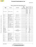
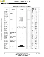
LSR opr8a
LSRA
LSRX
LSR oprx8,X
LSR ,X
LSR oprx8,SP
Logical Shift Right
– –
0
DIR
INH
INH
IX1
IX
SP1
34
44
54
64
74
9E64
dd
ff
ff
4
1
1
4
3
5
MOV opr8a,opr8a
MOV opr8a,X+
MOV #opr8i,opr8a
MOV ,X+,opr8a
Move
(M)
destination
←
(M)
source
H:X
←
(H:X) + $0001 in
IX+/DIR and DIR/IX+ Modes
0
–
–
–
DIR/DIR
DIR/IX+
IMM/DIR
IX+/DIR
4E
5E
6E
7E
dd dd
dd
ii dd
dd
5
4
4
4
MUL
Unsigned multiply
X:A
←
(X)
×
(A)
–
0
–
–
–
0 INH
42
5
NEG opr8a
NEGA
NEGX
NEG oprx8,X
NEG ,X
NEG oprx8,SP
Negate
(Two’s Complement)
M
←
– (M) = $00 – (M)
A
←
– (A) = $00 – (A)
X
←
– (X) = $00 – (X)
M
←
– (M) = $00 – (M)
M
←
– (M) = $00 – (M)
M
←
– (M) = $00 – (M)
– –
DIR
INH
INH
IX1
IX
SP1
30
40
50
60
70
9E60
dd
ff
ff
4
1
1
4
3
5
NOP
No Operation
Uses 1 Bus Cycle
–
–
–
–
–
–
INH
9D
1
NSA
Nibble Swap
Accumulator
A
←
(A[3:0]:A[7:4])
–
–
–
–
–
–
INH
62
3
ORA #opr8i
ORA opr8a
ORA opr16a
ORA oprx16,X
ORA oprx8,X
ORA ,X
ORA oprx16,SP
ORA oprx8,SP
Inclusive OR Accumulator
and Memory
A
←
(A) | (M)
0
–
–
–
IMM
DIR
EXT
IX2
IX1
IX
SP2
SP1
AA
BA
CA
DA
EA
FA
9EDA
9EEA
ii
dd
hh ll
ee ff
ff
ee ff
ff
2
3
4
4
3
2
5
4
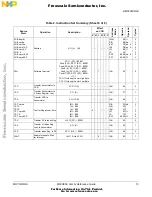
PSHA
Push Accumulator onto
Stack
Push (A); SP
←
(SP
) –
$0001
–
–
–
–
–
– INH
87
2
PSHH
Push H (Index Register
High) onto Stack
Push (H)
;
SP
←
(SP
) –
$0001
–
–
–
–
–
–
INH
8B
2
PSHX
Push X (Index Register
Low) onto Stack
Push (X)
;
SP
←
(SP
) –
$0001
–
–
–
–
–
–
INH
89
2
PULA
Pull Accumulator from
Stack
SP
←
(SP +
$0001); Pull
(
A
)
–
–
–
–
–
–
INH
86
2
PULH
Pull H (Index Register
High) from Stack
SP
←
(SP +
$0001); Pull
(
H
)
–
–
–
–
–
–
INH
8A
2
PULX
Pull X (Index Register
Low) from Stack
SP
←
(SP +
$0001); Pull
(
X
)
–
–
–
–
–
–
INH
88
2
ROL opr8a
ROLA
ROLX
ROL oprx8,X
ROL ,X
ROL oprx8,SP
Rotate Left through Carry
– –
DIR
INH
INH
IX1
IX
SP1
39
49
59
69
79
9E69
dd
ff
ff
4
1
1
4
3
5
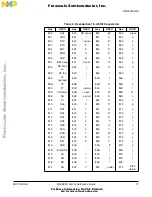
Table 2. Instruction Set Summary (Sheet 6 of 8)
Source
Form
Operation
Description
Effect
on CCR
Ad
dress
M
ode
Opc
o
de
O
p
erand
Cycl
es
V H I N Z C
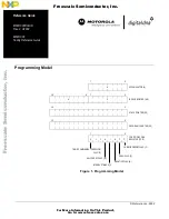
b0
b7
C
0
C
b0
b7
F
re
e
sc
a
le
S
e
m
ic
o
n
d
u
c
to
r,
I
Freescale Semiconductor, Inc.
For More Information On This Product,
Go to: www.freescale.com
n
c
.
..


