


Chapter 7 Background Debug Module (S12XBDMV2)
MC9S12XE-Family Reference Manual Rev. 1.19
Freescale Semiconductor
279
7.1.2.3
Low-Power Modes
The BDM can be used until all bus masters (e.g., CPU or XGATE or others depending on which masters
are available on the SOC) are in stop mode. When CPU is in a low power mode (wait or stop mode) all
BDM firmware commands as well as the hardware BACKGROUND command can not be used
respectively are ignored. In this case the CPU can not enter BDM active mode, and only hardware read and
write commands are available. Also the CPU can not enter a low power mode during BDM active mode.
If all bus masters are in stop mode, the BDM clocks are stopped as well. When BDM clocks are disabled
and one of the bus masters exits from stop mode the BDM clocks will restart and BDM will have a soft
reset (clearing the instruction register, any command in progress and disable the ACK function). The BDM
is now ready to receive a new command.
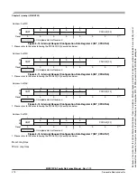
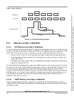
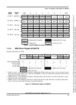
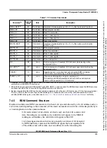
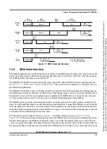
7.1.3
Block Diagram
A block diagram of the BDM is shown in
.
Figure 7-1. BDM Block Diagram
7.2
External Signal Description
A single-wire interface pin called the background debug interface (BKGD) pin is used to communicate
with the BDM system. During reset, this pin is a mode select input which selects between normal and
special modes of operation. After reset, this pin becomes the dedicated serial interface pin for the
background debug mode.
ENBDM
CLKSW
BDMACT
TRACE
SDV
16-Bit Shift Register
BKGD
Host
System
Serial
Interface
Data
Control
UNSEC
Register Block
Register
BDMSTS
Instruction Code
and
Execution
Standard BDM Firmware
LOOKUP TABLE
Secured BDM Firmware
LOOKUP TABLE
Bus Interface
and
Control Logic
Address
Data
Control
Clocks
Because
of
an
order
from
the
United
States
International
Trade
Commission,
BGA-packaged
product
lines
and
part
numbers
indicated
here
currently
are
not
available
from
Freescale
for
import
or
sale
in
the
United
States
prior
to
September
2010:
S12XE
products
in
208
MAPBGA
packages