Contetns
eLR100-UL-00 Manual for Consumer Products, Rev. 0.2, 02/2020
18 | 24
4.3.2.
Antenna Reference Trace Design
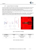
RF traces from eLR100‐UL‐00 module pads pin 47 and J2 pin 1 to the antenna must be made using micro‐strip traces.
This micro‐strip trace must respect the design of the Gerber file associated with the following figures in order to
obtain a uniform transmission line with a characteristic impedance of 50 ohms.
The reference trace design is shown as the green trace along with the side copper filled with vias on the left side.
of Figure where components C6, C7 are not installed; they were options on the reference board for future uses;
these uses are not FCC authorized yet.
As preliminary information the traces width of all sections are all 0.5mm and the length of eLR100‐UL‐00 pad to J2
connector are 6.2mm; However, refer to associated Gerber files for more details on dimensions and refer to
EWBM Inc for more details on the Gerber files. Table 1 shows the parts used in the reference trace design.
Figure 17. Antenna Reference Trace Design
Part Number
Reference
Description
Manufacture
LQP03TN10NH02D
R10
10nH, 3%
Murata
SMA‐4R‐PCB(1.8T)
J2
SMA, Subminiature Coaxial
Connector 50 ohm
Sungjin
N/A
C6, C7
Not Installed
N/A
Table 1. Antenna Micro‐strip Trace Parts

