


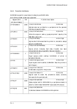

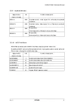

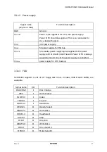


CARD-PCI/GX Hardware Manual
EPSON
Rev.A
36
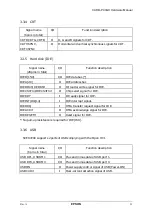
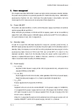
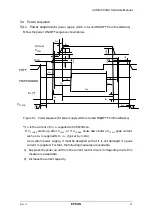
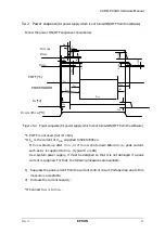
3.3.11 Power management
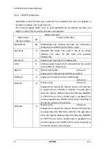
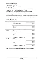
SCE8720C provides the following signals in order to achieve power supply control
complying ACPI.
Other than these signals, SCE8720C also provides signals to use BIOS ROM (ROMDIS).
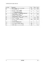
Signal name
(22 pins in total)
I/O
Function description
POFF
OD
Output signal which controls ON/OFF of the power
supply. Power OFF at HIGH, and ON at LOW.
PWSW#
I
Input signal of the power ON/OFF switch.
STANDBY#
OD
Output signal which represents standby status.
Standby at LOW.
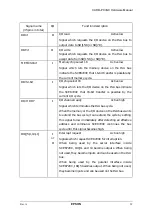
POWERGOOD
I
Input power good signal which indicates that the power
is properly supplied. When this signal is LOW, the card
is initialized.
PME1#
I
Wake on RING input
PME0#
I
Power management input signal usually assigned to
Wake on LAN signal.
PORT4
programmable General-purpose input/output signal.
(GPIO13 of PC97317)
PORT3
programmable General-purpose input/output signal.
(GPIO12 of PC97317)
CPUFRQ
I
Input signal. Set it to NC with SCE8720Cxx.
ROMDIS
I
Input signal. Disable signal of ROM inside SCE8720C.
CPU accesses the external ROM when the signal is
HIGH, and internal ROM when LOW.
RESERVED
---
RESERVED pin. Set it to NC.


