Embedded Solutions
Page 5
figures 2 & 3 at the rear of this manual.
Install the RP/RX resistors to tie the XMC signal to the selection point – to distribute to
the SCSI or DIN connector and or other XMC position. Use RCB and/or RIO to select
the IO side of the connection. This “I” form made of 4 0402 resistors allows for selection
with almost no signal stub. Selectable on a signal by signal basis.
Special features
:
• 24 lane Gen1/2 compliant Switch
• 8 lanes allocated to PCIe “gold finger” interface. 8 lanes each to the XMC’s
• Switch can store and forward locally to communicate directly between the XMC’s
• Voltage monitors, each with LED’s on plus 12V, minus 12V, plus 5V, plus 3.3V, and
switch power [1.0V]
• 10A regulator for XMC 3.3V and 5V supplies. Shunts for Delayed, not Delayed, Off
• Selection switch for VPWR [12V or 5V] per XMC. Option for hardwired 5V or 12V
• Front panel connector access through PCI bracket
• User IO [Jn4 and/or Jn6] available through one of two cable connectors (DIN IDC or
SCSI II compatible) Spare pins on SCSI connector can be shunt selected to power
or ground.
• Connector Bus available to cross connect XMC rear IO between modules
• Cooling cutout for increased airflow to XMC’s
• Optional Fan(s) for increased airflow
• JTAG programming support
• DIP switch to select global addressing on XMC’s
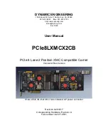
The PCIe8LXMCX2CB is ready to use with the default settings. Just install the XMC(s)
onto PCIe8LXMCX2CB and then into the system.
RP
RX
RIO
RCB
SCSI/DIN
XMC
JN6
JN4


