Specifications subject to change without notice
© Digital View Ltd – Doc Ver 1.5: 27 March 2012 (SGX-1920L_manual.doc)
Page
50 of 60
Appendix III – Mapping definition
•
Definition of Mapping A :
Страница 1: ...controller 13 Connectors pinouts jumpers Essential connection information 25 Controller dimensions 27 Application notes 29 Troubleshooting 30 Specifications 31 Appendix I Supported graphics modes tabl...
Страница 2: ...3 P N 4160196xx 3 PR 2400 P N 41601951x 3 P N 4160195xx 3 HOW TO PROCEED Ensure you have all parts that they are correct refer to Connection diagram Connector reference in following section Assembly...
Страница 3: ...7 OSD Function controls cable 8 Status LED optional 9 IR sensor optional 10 RS 232 control interface 11 Secondary RS 232 control interface 12 External panel power output 13 Audio adaptor board optiona...
Страница 4: ...rrect cable pin out to match inverter Using wrong cable pin out may damage the inverter 6 Function Controls The following section discusses the controls required and the section on connectors provides...
Страница 5: ...he board is not user serviceable or repairable Warranty does not cover user error in connecting up to the controller and is invalidated by unauthorized modification or repairs Controller Mounting It i...
Страница 6: ...pay attention to the settings of JA3 JA6 on SGX 1920L JB2 and JB3 on PR 1200 PR 2400 JB2 JB3 are used for inverter control read inverter specification and information on the jumper table to define th...
Страница 7: ...will auto time off Back to previous OSD menu page Menu button Menu button Select down Moves the selector to the next function down SEL DN SEL DN Select up Moves the selector to the previous function u...
Страница 8: ...e fill screen expansion for lower resolution image according to aspect ratio 4 3 scaling format in 4 3 16 9 scaling format in 16 9 16 10 scaling format in 16 10 2 35 1 scaling format in 2 35 1 2 1 sca...
Страница 9: ...ally OFF PIP window keeps on DISPLAY WHEN SETTING ON UNDER SETUP AUTO SOURCE SEEK Utilities Setup 4 Auto Picture Setup Auto adjust the image position phase and size Auto Color Gain Auto Color Calibrat...
Страница 10: ...ff Safe Area Marker 80 99 Aspect Marker 4 3 16 9 Transparency Level 0 25 50 75 100 Exit menu Language English Spanish French German Chinese Select OSD menu language display Transparency OFF ON Set OSD...
Страница 11: ...ll color temperature settings to the default values Hot Key 4 Hot key 1 Volume Brightness Contrast Inputs Aspect Ratio Zoom Freeze PIP Size PIP Swap Saturation Hue Backlight Auto Picture Setup Markers...
Страница 12: ...Factory Defaults with Color Temp 4 Activate when JC1 position 4 sets open Are you sure Yes No Save Current Settings as Calibrated Values 4 Activate when JC1 position 2 sets closed Are you sure Yes No...
Страница 13: ...nector Molex 53261 0571 Matching type Molex 51021 0500 Matching connection cable P N 426031600 3 CN10 HDMI audio Stereo output JST S4B ZR SM4A Matching type JST ZHR 4 Matching connection cable P N 426...
Страница 14: ...signal High 5V 1 2 On Off control signal High 3 3V Open On Off control signal High Open collector CAUTION Incorrect setting can damage inverter JB3 Backlight inverter on off control polarity 1 2 cont...
Страница 15: ...compatible Matching connector type Molex 43025 0400 compatible Matching power cable P N 426013700 3 PP2 Power input PR 1200 12VDC power input PR 2400 24VDC power input Molex 43650 0200 compatible Mat...
Страница 16: ...5V 5V 1 3 2 4 12VDC 12V OPEN 5 7 6 8 CAUTION Incorrect setting can damage panel controller Table 2 PR 2400 Panel voltage setting table Input voltage via PP2 or PP3 Panel Voltage JA3 JA6 Jumper on boar...
Страница 17: ...ect to change without notice Digital View Ltd Doc Ver 1 5 27 March 2012 SGX 1920L_manual doc Page 17 of 60 JA3 JA6 location on board Please pay attention to the jumper settings on JA3 JA6 which are re...
Страница 18: ...A320W2 L01 LTA230W1 L02 1366x768 ON ON ON ON NEC NL12876BC26 21 Samsung LTM170W1 L01 1280x768 OFF ON ON ON CHI MEI N154I4 L01 1280x800 OFF OFF ON OFF AU Optronics M190PW01 1440x900 OFF OFF ON ON Sharp...
Страница 19: ...ction ON LVDS panel OFF Reserved 4 LVDS data mapping select Refer to Table 2 If SW4 position 5 OFF 8 bit OFF Mapping B ON Mapping A Please adjust to get the correct picture See as Appendix I for detai...
Страница 20: ...rved 3 VCC 5V 4 TXD RS 232 Tx data 5 GND Ground 6 RXD RS 232 Rx data CN9 Ambient light sensor connector Molex 53261 0571 Matching type Molex 51021 0500 PIN SYMBOL DESCRIPTION 1 IP1 Reserved 2 IP2 Rese...
Страница 21: ...2 GND Ground 3 IN_VGA1_G Green analog 1 4 GND Ground 5 IN_VGA1_B Blue analog 1 6 GND Ground 7 IN_VGA1_HS Horizontal sync or composite sync input 1 8 GND Ground 9 IN_VGA1_VS Vertical sync input 1 10 G...
Страница 22: ...DATA1 TMDS Data 1 38 DATA2 TMDS Data 2 39 DATA2S TMDS Data 2 Shield 40 DATA2 TMDS Data 2 41 GND Ground J2 Additional panel power input connector Molex 53261 0871 Matching type Molex 51021 0800 PIN SY...
Страница 23: ...ial LVDS data bit B3 41 GND Ground 42 TXBC Positive LVDS clock for B channel 43 TXBC Negative LVDS clock for B channel 44 GND Ground 45 TXB2 Positive differential LVDS data bit B2 46 TXB2 Negative dif...
Страница 24: ...8 PIN SYMBOL DESCRIPTION 1 PVLCD Panel power supply 3 3V 5V 2 PVLCD Panel power supply 3 3V 5V 3 GND Ground 4 GND Ground 5 GND Ground 6 PVLCD12 Panel power supply 12V selected by JA3 JA6 7 PVLCD12 Pa...
Страница 25: ...e controller is 17 65mm with or without video add on board measured from bottom of PCB to top of components including any underside components leads We recommend clearances of 5mm from bottom of PCB i...
Страница 26: ...g any underside components leads We recommend clearances of 5mm from bottom of PCB if mounting on a metal plate we also recommend a layer of suitable insulation material is added to the mounting plate...
Страница 27: ...ched with the inverter specification see table CNB1 PIN DESCRIPTION 1 Ground 2 PR 1200 12VDC PR 2400 24VDC Remark For higher power inverter more current for 12V 24V can be taken from CNA1 pin 1 Enable...
Страница 28: ...ess depends on the inverter The main power load for On Off is handled by a relay on the controller Example for circuit design Signal description Notes 1 R1 470ohm on board 2 RPOT is an external potent...
Страница 29: ...cting the signal such as a signal splitter please note that normally a signal splitter will not have any adverse effect Image appearance A faulty panel can have blank lines failed sections flickering...
Страница 30: ...RGB ARGB 2 Composite video 1 Composite video 2 Composite video 3 Composite video 4 HDMI 1 HDMI 2 Functions display On screen display OSD of functions OSD menu functions Image controls Panel brightness...
Страница 31: ...0 Digital Separate Sync V_75 640x480 75Hz 31 500 37 500 75 000 Sync On Green V_75 640x480 75Hz 31 500 37 500 75 000 Composite Sync SV_56 800x600 56Hz 36 000 35 156 56 250 Digital Separate Sync SV_56 8...
Страница 32: ...SX_75 1280x1024 75Hz 135 79 976 75 Digital Separate Sync SX_75 1280x1024 75Hz 135 79 976 75 Sync On Green SX_75 1280x1024 75Hz 135 79 976 75 Composite Sync UX_60 1600x1200 60Hz 162 75 000 60 Digital...
Страница 33: ...MHz Horizontal freq KHz Vertical freq Hz T_70 720x400 70Hz 28 322 31 469 70 087 V_60 640x480 60Hz 25 175 31 469 59 940 SV_60 800x600 60Hz 40 000 37 879 60 317 X_60 1024x768 60Hz 65 000 48 363 60 004 S...
Страница 34: ...lex 51021 0600 Mating connector DB9 Female PIN Description PIN Description 4 RS 232 Tx Data 2 RS 232 Rx Data 5 Ground 3 RS 232 Tx Data 6 RS 232 Rx Data 5 Ground Software connection The OSD function ca...
Страница 35: ...rightness value increment decrement Reset Query Current Source Maximum query 1 Minimum query 1 Set Source value 1 Query Source 1 Brightness Range 4 E B 2 Default 8 0 ss reference by Input main select...
Страница 36: ...D V position 0x91 nnn r R Set osd_vpos value increment decrement Reset Query OSD vertical position Range 0 0 F F Default 8 0 OSD Transparency 0x92 n r R Set OSD transparency value increment decrement...
Страница 37: ...1 NTSC_M_358 2 PAL_N_443 3 SECAM 4 NTSC_M_443 5 PAL_M_358 7 PAL_M_443 9 PAL_N_358 Video State Query 0 No video 1 NTSC 2 PAL 3 SECAM 4 NTSC 443 5 PAL M 358 GAMMA value select 0x9d n r R Select GAMMA v...
Страница 38: ...5 5 PIP V position 0xa5 nnn r R Set PIP_vpos value increment decrement Reset Query PIP window vertical position Range 0 0 0 0 6 4 Default 0 1 4 PIP window size select 0xa6 nn r R Select PIP window si...
Страница 39: ...value of H Size V Size and input resolution Vertical Pan 0xb2 nnn r R Set Vertical pan position for Aspect Size value increment decrement Reset Query Scalar vertical pan position PAL 576i NTSC 480i A...
Страница 40: ...n horizontal frequency Graphic vertical sync frequency enquiry 0xba Vertical sync frequency in units of Hz in 3 digit hex number and 1 char nnnn vertical frequency nnn 3 digit hex c i or p interlace o...
Страница 41: ...uery Color Monochrome mode selection Output Channel Select 0xe2 0 1 2 3 4 5 6 R r Off Blue Only Red Only Green Only Blue Mono Red Mono Green Mono 0 Off 1 Blue Only 2 Red Only 3 Green Only 4 Blue Mono...
Страница 42: ...ffset for selected colour temperature 0xea nn r R m n i ss c nn o ss c Set the Offset of the blue channel for the selected colour temp value increment decrement Reset Query Maximum query 1 Minimum que...
Страница 43: ...On 0 Off 1 On Display real time clock 0xee 0x4D 0 1 Real Time Clock Display Off Real Time Clock Display 0 Off 1 On Custom Sizing 0xef 0 1 2 Custom sizing selection Overscan Normal Custom Query 0 Over...
Страница 44: ...command acknowledge 0 acknowledge disabled 1 acknowledge enabled Auto setup 0xc3 Start auto setup of current vmode 0 fail 1 successful Command availability 0xc4 n Check whether a command is available...
Страница 45: ...ated default 0xd7 Saving all parameters to user default value 1 successful Load Calibrated default 0xd8 Loading all parameters to user default value 1 successful 0 not successful E Checksum Error Wide...
Страница 46: ...64 0x20 0x54 0x65 0x78 0x74 0x0A 0x31 Clear Line 0xF0 C LL Return nn C 0x43 or 0x63 Clear command LL 0x30 0x31 0x30 0x34 Line number Rang 0 4 lines C Clear command LL Line Number nn Return Line number...
Страница 47: ...Return Value pixels e g Set Text Window Horizontal Size 640 pixels 0x280 HEX RS232 Code 0xF0 0x58 0x32 0x38 0x30 Return Code 0xF0 0x58 0x32 0x38 0x30 0x32 0x38 0x30 Background Transparency 0xF0 B N R...
Страница 48: ...0x48 or 0x68 nn 0x30 0x30 0x46 0x46 H Horizontal Position command ss Set Horizontal Position number nn Return Position number e g Set Display Mark Horizontal Position RS232 Code 0xF1 0x48 0x30 0x31 R...
Страница 49: ...meter value of 0x1e is represented by 1 e E 0x31 0x6e 0x4e Please refer to the ASCII to Hex convert table below Hex to ASCII conversion table Hex ASCII Hex ASCII Hex ASCII Hex ASCII 0x30 0 0x41 A 0x61...
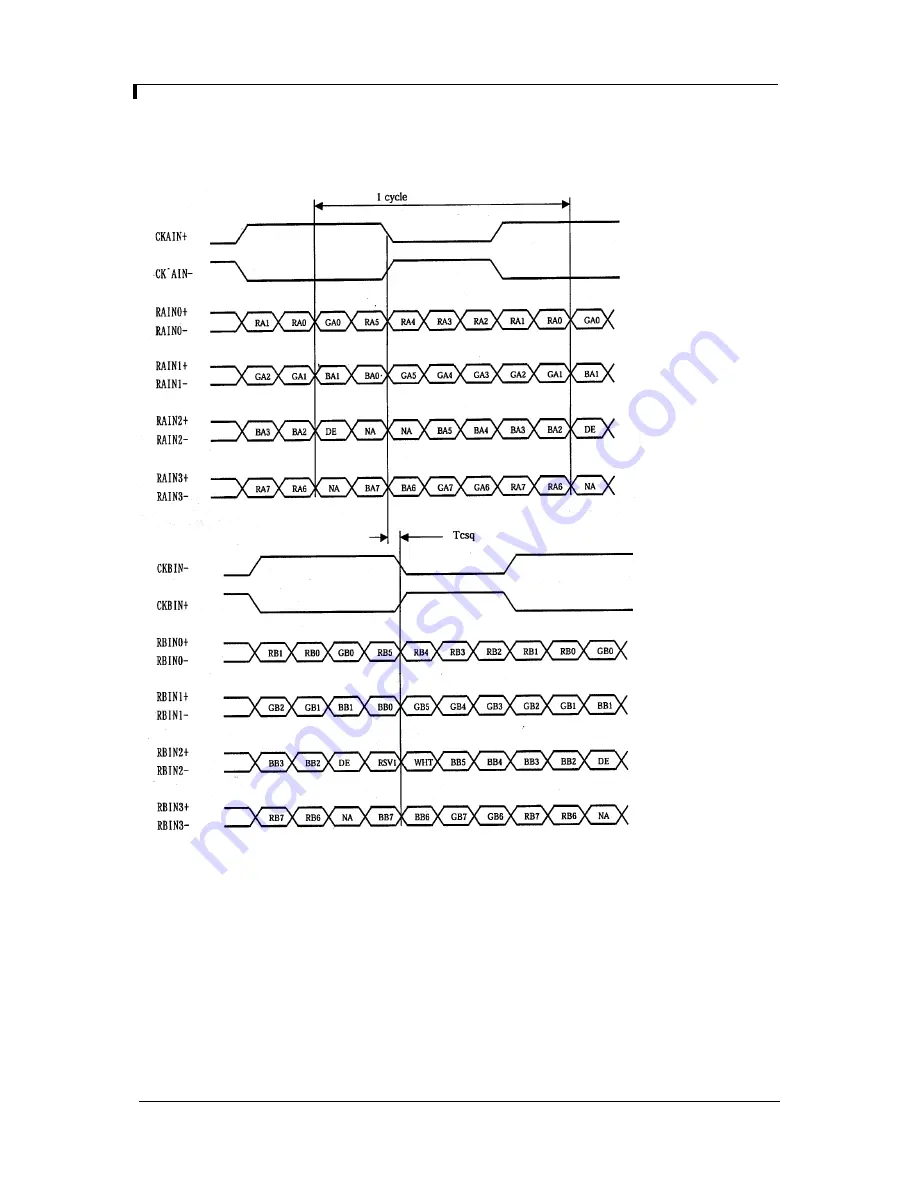
Страница 50: ...Specifications subject to change without notice Digital View Ltd Doc Ver 1 5 27 March 2012 SGX 1920L_manual doc Page 50 of 60 Appendix III Mapping definition Definition of Mapping A...
Страница 51: ...Specifications subject to change without notice Digital View Ltd Doc Ver 1 5 27 March 2012 SGX 1920L_manual doc Page 51 of 60 Definition of Mapping B...
Страница 52: ...Specifications subject to change without notice Digital View Ltd Doc Ver 1 5 27 March 2012 SGX 1920L_manual doc Page 52 of 60 Definition of VESA...
Страница 53: ...Specifications subject to change without notice Digital View Ltd Doc Ver 1 5 27 March 2012 SGX 1920L_manual doc Page 53 of 60 Definition of JEIDA...
Страница 54: ...ected by the Reset Factory Defaults function The reference pattern can be downloaded at http www digitalview com support downloads TestPattern_1280 BMP This reference pattern is for 1280x1024 resoluti...
Страница 55: ...lume BUTTON Use this button to direct control the hotkey function Press the button to increase the pre set hotkey parameter value and the button to decrease the pre set hotkey parameter value In OSD m...
Страница 56: ...ing too fast it will have image artifact and get worst quality MADI Motion adaptive de interlacing It is a pixel based method which used for the input fields have no fixed relation between them If the...
Страница 57: ...0 to 21 dB Use of connectors Connector Connector type CN1 JST B3B XH A CN2 JST B4B PH K CN3 0 1 inches 2 row x 5 pin header strips right angle J1 3 5mm stereo jack socket J2 3 5mm stereo jack socket...
Страница 58: ...X 1920L_manual doc Page 58 of 60 CN3 Controller interface connector Pin Number Description 1 5V 2 Left trimpot chip select 3 Right trimpot chip select 4 Trimpot serial data 5 Trimpot serial clock 6 Di...
Страница 59: ...s on products furnished hereunder including all implied warranties of merchantability and fitness for a particular application or purpose The stated express warranties are in lieu of all obligations o...
Страница 60: ...g 130 Morgan Hill California 95037 USA Tel 1 408 782 7773 Fax 1 408 782 7883 Sales ussales digitalview com EUROPE Digital View Ltd The Lake House Knebworth Park Herts SG3 6PY UK Tel 44 0 20 7631 2150...
Страница 61: ...Mouser Electronics Authorized Distributor Click to View Pricing Inventory Delivery Lifecycle Information Digital View 426031600 3...