


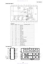
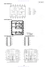
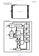
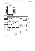
10
DHT-500SD
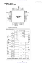
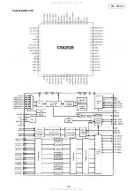
Description
Pin No.
Pin Name
Type
97
XHPDIAGJ
I/O
This pin is used as the Passed Diagnostics signal, and may be an input or an open-drain output
92
XHDASPJ
I/O
This pin is used as the Drive Active/Slave Present signal, and is an input or an open-drain
output. This pin is used for Master/Slave drive communication and/or for driving an LED
102
XHIORDY
I/O
1. I/O channel ready. This signal is driven low to extend host transfer cycles when the controller
is not ready to respond. This pin will be tri-stated when a read or write is not in progress.
2. MPEG error. This pin is used as the ERROR signal when MPEG interface mode is selected
95, 96, 98
XHA[2:0]
I
Host address lines. The host address lines A[2:0] are used to access the various host control,
status, and data registers
XHD[15.0]
I/O
1. Host data bus. This bus is used to transfer data and status between the host and the controller.
106, 107, 108,
2. MPEG data bus 7-8. The HD[7:0] are used as the DATA [7:0] when MPEG interface mode is selected.
109, 111, 112,
3. VCD I/F. Bit3-0 are used as VCD I/F signal when VCD function is enabled. The relationship of
113, 114, 116,
bit3-0 and VCD I/F is as follow
117, 118, 119,
HD0—CD-DATA
120, 121, 122,
HD1—CD-LRCK
123
HD2—CD-BCK
HD3—CD-C2PO
143
XRSDCLK
O
This signal is the clock output for SDRAM
147
XROEJ
O
This signal is used as the memory output enable for external DRAM buffers. After RSTJ is
asserted, this signal will be low
142
XRWEJ
O
This signal is asserted low when a buffer memory write operation is active
144
XRRASJ
O
This signal is used as Row address output to external DRAM buffer. After RSTJ is asserted, this
signal will be high
145
XRCASJ
O
This signal is used as column address output to external DRAM. After RSTJ is asserted, this
signal will be high
1. RAM address lines. These are bits11-0 for addressing the buffer memory.
2. Hardware setting. The bits6-0 are used as hardware setting for some functions.
RA[9] : FLASH size is 64K/128K
1:
FLASH size is 64K
0:
FLASH size is 128K
RA[8] : External CPU is 8032/H8
1:
8032
0:
H8
RA[7] : Microcontroller programmable I/O port 1 pin control
1:
By internal microcontroller
148, 149, 151,
0:
By registers to decide input/output
152, 153, 155,
RA[6] : System test pin output
156, 157, 158, XRA[11:0]
O
1:
Normal operation
159, 160, 161
0:
System test pin output
RA[5] : For testing purpose, don’t need to set
RA[4] : IDE master/slave
1:
Slave
0:
Master
RA[3] : For testing purpose, don’t need to set
RA[2] : For testing purpose, don’t need to set
RA[1-0] : MCU Mode selection
11: Normal Mode (internal uP, internal address latch)
10: Outside uP Mode (ICE Mode)
01: Test mode for internal uP testing
00: Internal uP mode with external address latch
124, 125, 126,
XRD[15:0]
I/O
These signals are the 8-bit parallel data lines to/from the buffer memory.
127, 128, 129,
131, 132, 134,
135, 136, 137,
138, 139, 140,
141
4
Analog Power +5V for Data Slicer part
Analog Power +5V for DAC part
Analog Power +5V for ADC part
Analog Power +5V for Data PLL part
Power +3.3V for digital core logic and pad
Analog Ground for Data Slicer part
Analog Ground for DAC part
Analog Ground for ADC part
Analog Ground for Data PLL part
Digital Ground core logic and pad.
www. xiaoyu163. com
QQ 376315150
9
9
2
8
9
4
2
9
8
TEL 13942296513
9
9
2
8
9
4
2
9
8
0
5
1
5
1
3
6
7
3
Q
Q
TEL 13942296513 QQ 376315150 892498299
TEL 13942296513 QQ 376315150 892498299


