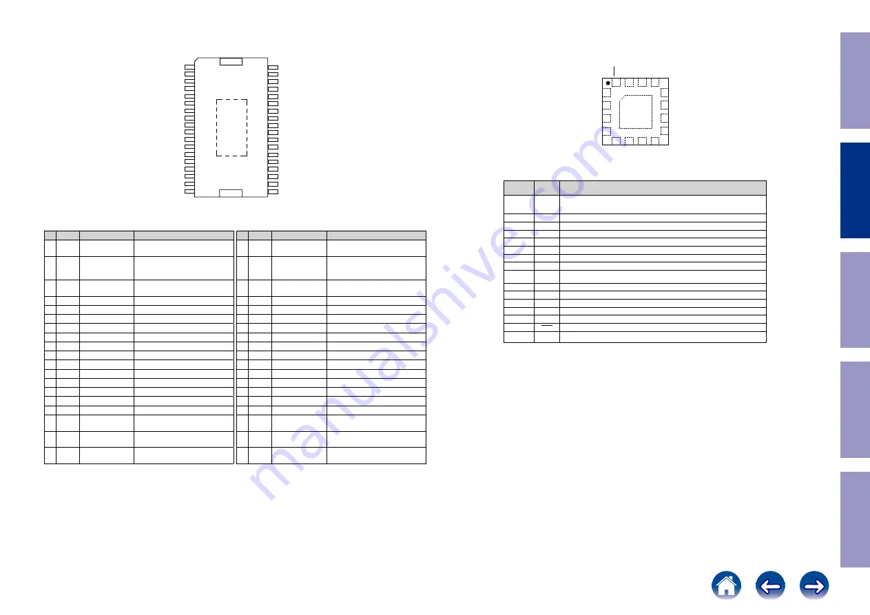
STA339BWS (U19 : STA339BW)
Pin function
Pin Type
Name
Description
Pin Type
Name
Description
1
GND GND_SUB
Substrate ground
19
O
EAPD / OUT4B
Power down for external bridge /
PWM out channel 4B
2
I
SA
I2C select address (pull-down)
20
I/O
TWARN / OUT4A
"Thermal warning from external
bridge (pull-up when input)
/ PWM out channel 4A"
3
I
TEST_MODE
This pin must be connected to
ground (pull-down)
21 Power VDD_DIG
Digital supply voltage
4
I/O
VSS
Internal reference at VCC - 3.3 V
22 GND GND_DIG
Digital ground
5
I/O
VCC_REG
Internal VCC reference
23
I
PWRDN
Power down (pull-up)
6
O
OUT2B
Output half-bridge channel 2B
24 Power VDD_PLL
Positive supply for PLL
7
GND GND2
Power negative supply
25
I
FILTER_PLL
Connection to PLL filter
8 Power VCC2
Power positive supply
26 GND GND_PLL
Negative supply for PLL
9
O
OUT2A
Output half-bridge channel 2A
27
I
XTI
PLL input clock
10
O
OUT1B
Output half-bridge channel 1B
28
I
BICKI
I2S serial clock
11 Power VCC1
Power positive supply
29
I
LRCKI
I2S left/right clock
12 GND GND1
Power negative supply
30
I
SDI
I2S serial data channels 1 and 2
13
O
OUT1A
Output half-bridge channel 1A
31
I
RESET
Reset (pull-up)
14 GND GND_REG
Internal ground reference
32
O
INT_LINE
Fault interrupt
15 Power VDD
Internal 3.3 V reference voltage
33
I/O
SDA
I2C serial data
16
I
CONFIG
Parallel mode command
34
I
SCL
I2C serial clock
17
O
OUT3B / FFX3B
PWM out channel 3B / external
bridge driver
35 GND GND_DIG
Digital ground
18
O
OUT3A / FFX3A
PWM out channel 3A / external
bridge driver
36 Power VDD_DIG
Digital supply voltage
-
-
EP
Exposed pad for PCB heatsink, to
be connected to GND
1
2
3
4
5
6
7
8
9
10
11
12
13
14
15
16
17
18
36
35
34
33
32
31
30
29
28
27
26
25
24
23
22
21
20
19
VDD_DIG
GND_DIG
SCL
SDA
INT_LINE
RESET
SDI
LRCKI
BICKI
XTI
GND_PLL
FILTER_PLL
VDD_PLL
PWRDN
GND_DIG
VDD_DIG
TWARN / OUT4A
EAPD / OUT4B
GND_SUB
SA
TEST_MODE
VSS
VCC_REG
OUT2B
GND2
VCC2
OUT2A
OUT1B
VCC1
GND1
OUT1A
GND_REG
VDD
CONFIG
OUT3B / FFX3B
OUT3A / FFX3A
EP, exposed pad
(device ground)
SGM4917 (U24 : HP_AMP)
Pin function
(TOP VIEW)
OUTR
SV
DD
OUTL
INL-
SV
SS
INL+
PV
SS
C1N
PGND
C1P
INR+
SGND
INR-
PV
DD
TQFN-3×3-16L
SV
DD
SHDN
9
12
11
10
5
6
7
8
16
15
14
13
4
1
2
3
PIN
NAME
DESCRIPTION
1
PV
DD
Charge-Pump Power Supply. Powers charge-pump inverter, charge-pump logic, and oscillator.
Connect to positive supply (2.7V to 5.5V). Bypass with a 1µF capacitor to PGND as close to the
pin as possible.
2
C1P
Flying Capacitor Positive Terminal.
3
PGND
Power Ground. Connect to ground.
4
C1N
Flying Capacitor Negative Terminal.
5
PV
SS
Charge-Pump Output. Connect to SV
SS
.
6
SGND
Signal Ground. Connect to ground.
7
INR+
Noninverting Right-Channel Audio Input.
8
INR-
Inverting Right-Channel Audio Input.
9,13
SV
DD
Amplifier Positive Power Supply. Connect to positive supply (2.7V to 5.5V). Bypass with a 1µF
capacitor to SGND as close to the pin as possible.
10
OUTR
Right-Channel Output.
11
SV
SS
Amplifier Negative Power Supply. Connect to PV
SS
.
12
OUTL
Left-Channel Output.
14
INL-
Inverting Left-Channel Audio Input.
15
INL+
Noninverting Left-Channel Audio Input.
16
SHDN
Active-Low Shutdown Input.
Exposed
Paddle
‒
Exposed Paddle. Can be connected to GND or left floating.
Before Servicing
This Unit
Electrical
Mechanical
Repair Information
Updating
27


