background image

Chapter 4

Signal Connections

©

 National Instruments Corporation

4-29

PCI-MIO E Series User Manual

EXTSTROBE* Signal

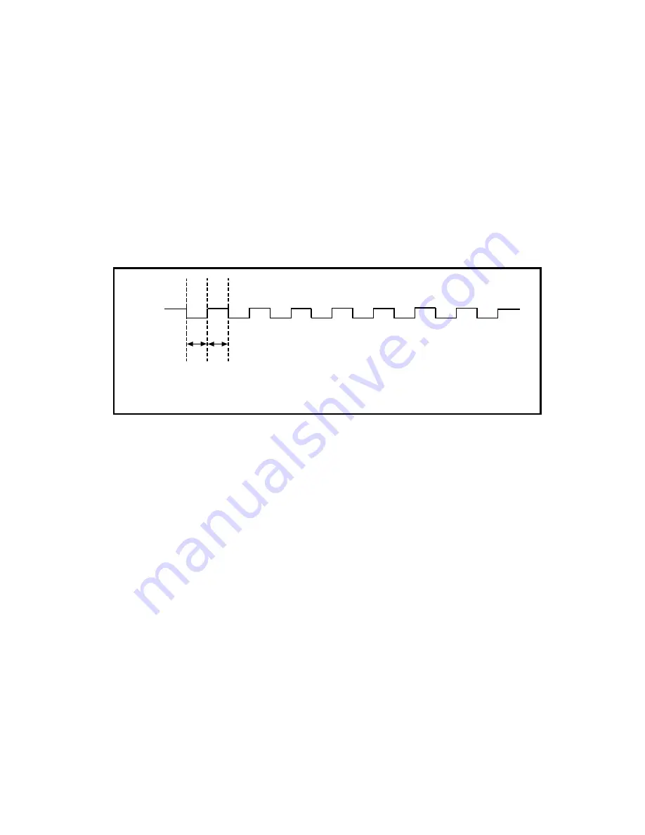
EXTSTROBE* is an output-only signal that generates either a single 

pulse or a sequence of eight pulses in the hardware-strobe mode. An 
external device can use this signal to latch signals or to trigger events. 
In the single-pulse mode, software controls the level of the 
EXTSTROBE* signal. A 10 

µ

s and a 1.2 

µ

s clock are available for 

generating a sequence of eight pulses in the hardware-strobe mode. 
Figure 4-14 shows the timing for the hardware-strobe mode 
EXTSTROBE* signal.

Figure 4-14.  EXTSTROBE* Signal Timing

TRIG1 Signal

Any PFI pin can externally input the TRIG1 signal, which is available 

as an output on the PFI0/TRIG1 pin. 

Refer to Figures 4-11 and 4-12 for the relationship of TRIG1 to the 

DAQ sequence.

As an input, the TRIG1 signal is configured in the edge-detection mode. 

You can select any PFI pin as the source for TRIG1 and configure the 
polarity selection for either rising or falling edge. The selected edge of 
the TRIG1 signal starts the data acquisition sequence for both 
posttriggered and pretriggered acquisitions. The PCI-MIO-16E-1, 
PCI-MIO-16E-4, and PCI-MIO-16XE-10 support analog triggering on 
the PFI0/TRIG1 pin. See Chapter 3, Hardware Overview, for more 
information on analog triggering.


t w t w

VOH

VOL

t w = 600 ns or 5 

µ

s

Содержание DAQ PCI-MIO E Series

Страница 1: ...or PCI Bus Computers January 1997 Edition Part Number 320945B 01 Copyright 1995 1997 National Instruments Corporation All Rights Reserved Click here to comment on this document via the National Instru...

Страница 2: ...mark 45 76 26 00 Finland 09 527 2321 France 01 48 14 24 24 Germany 089 741 31 30 Hong Kong 2645 3186 Israel 03 5734815 Italy 02 413091 Japan 03 5472 2970 Korea 02 596 7456 Mexico 5 520 2635 Netherland...

Страница 3: ...NTAL OR CONSEQUENTIAL DAMAGES EVEN IF ADVISED OF THE POSSIBILITY THEREOF This limitation of the liability of National Instruments will apply regardless of the form of action whether in contract or tor...

Страница 4: ......

Страница 5: ...xiv Customer Communication xiv Chapter 1 Introduction About the PCI MIO E Series 1 1 What You Need to Get Started 1 2 Software Programming Choices 1 3 National Instruments Application Software 1 3 NI...

Страница 6: ...Signal Connections I O Connector 4 1 I O Connector Signal Descriptions 4 3 Analog Input Signal Connections 4 11 Types of Signal Sources 4 13 Floating Signal Sources 4 13 Ground Referenced Signal Sourc...

Страница 7: ...iming Connections 4 37 WFTRIG Signal 4 37 UPDATE Signal 4 38 UISOURCE Signal 4 40 General Purpose Timing Signal Connections 4 40 GPCTR0_SOURCE Signal 4 41 GPCTR0_GATE Signal 4 42 GPCTR0_OUT Signal 4 4...

Страница 8: ...s Analog Triggering Mode 3 15 Figure 3 10 Low Hysteresis Analog Triggering Mode 3 15 Figure 3 11 CONVERT Signal Routing 3 17 Figure 3 12 RTSI Bus Signal Connection 3 19 Figure 4 1 I O Connector Pin As...

Страница 9: ...Signal Timing 4 39 Figure 4 28 UISOURCE Signal Timing 4 40 Figure 4 29 GPCTR0_SOURCE Signal Timing 4 41 Figure 4 30 GPCTR0_GATE Signal Timing in Edge Detection Mode 4 42 Figure 4 31 GPCTR0_OUT Signal...

Страница 10: ......

Страница 11: ...e analog input analog output digital I O and timing I O Organization of This Manual The PCI MIO E Series User Manual is organized as follows Chapter 1 Introduction describes the PCI MIO E Series board...

Страница 12: ...ere you can find the topic Conventions Used in This Manual The following conventions are used in this manual bold Bold text denotes parameters bold italic Bold italic text denotes a note caution or wa...

Страница 13: ...ting Started with SCXI If you are using SCXI this is the first manual you should read It gives an overview of the SCXI system and contains the most commonly needed information for the modules chassis...

Страница 14: ...alog Signals PCI Local Bus Specification Revision 2 0 The following National Instruments manual contains detailed information for the register level programmer PCI MIO E Series Register Level Programm...

Страница 15: ...completely switchless and jumperless data acquisition DAQ boards for the PCI bus This feature is made possible by the National Instruments MITE bus interface chip that connects the board to the PCI I...

Страница 16: ...AQ boards Detailed specifications of the PCI MIO E Series boards are in Appendix A Specifications What You Need to Get Started To set up and use your PCI MIO E Series board you will need the following...

Страница 17: ...series of VIs for using LabVIEW with National Instruments DAQ hardware is included with LabVIEW The LabVIEW Data Acquisition VI Library is functionally equivalent to NI DAQ software LabWindows CVI fea...

Страница 18: ...DAQ I O functions for maximum ease of use and low level DAQ I O functions for maximum flexibility and performance Examples of high level functions are streaming data to disk or acquiring a certain num...

Страница 19: ...ster level programming software can be very time consuming and inefficient and is not recommended for most users Even if you are an experienced register level programmer using NI DAQ or application so...

Страница 20: ...specific information about these products refer to your National Instruments catalogue or call the office nearest you Custom Cabling National Instruments offers cables and accessories for you to proto...

Страница 21: ...ntistatic package to prevent electrostatic damage to the board Electrostatic discharge can damage several components on the board To avoid such damage in handling the board take the following precauti...

Страница 22: ......

Страница 23: ...software packages refer to the appropriate release notes After you have installed your application software refer to your NI DAQ release notes and follow the instructions given there for your operatin...

Страница 24: ...now ready to configure your software Refer to your software documentation for configuration instructions Board Configuration Due to the National Instruments standard architecture for data acquisition...

Страница 25: ...NI PGIA Gain Amplifier Calibration Mux Mux Mode Selection Switches Analog Muxes Voltage REF Calibration DACs Dither Circuitry Trigger Analog Trigger Circuitry 2 Trigger Level DACs 6 Calibration DACs...

Страница 26: ...itches Analog Muxes Voltage REF Calibration DACs 4 Calibration DACs DAC0 DAC1 DAQ STC Analog Input Timing Control Analog Output Timing Control Digital I O Trigger Counter Timing I O RTSI Bus Interface...

Страница 27: ...FF input The single ended input configurations provide up to 16 channels The DIFF input configuration provides up to eight channels Input modes are programmed on a per Timing PFI Trigger I O Connector...

Страница 28: ...a positive reference voltage Bipolar input means that the input voltage range is between Vref 2 and Vref 2 The PCI MIO 16E 1 and PCI MIO 16E 4 have a unipolar input range of 10 V 0 to 10 V and a bipol...

Страница 29: ...ws the overall input range and precision according to the input range configuration and gain used Table 3 2 Actual Range and Measurement Precision PCI MIO 16E 1 and PCI MIO 16E 4 Range Configuration G...

Страница 30: ...gure each input channel uniquely Note You can calibrate your PCI MIO 16XE 10 and PCI MIO 16XE 50 analog input circuitry for either a unipolar or bipolar polarity If you mix unipolar and bipolar channe...

Страница 31: ...gnal will not be negative below 0 V unipolar input polarity is best However if the signal is negative or equal to zero you will get inaccurate readings if you use unipolar input polarity Table 3 3 Act...

Страница 32: ...educes measurement noise resulting in improved resolution For high speed applications not involving averaging or spectral analysis you may want to disable the dither to reduce noise Your software enab...

Страница 33: ...time for the very high speed boards is gain dependent which can affect the useful sampling rate for a given gain No extra settling time is necessary between channels as long as the gain is constant an...

Страница 34: ...pm or 1 400 LSB of the 4 V step It may take as long as 200 s for the circuitry to settle this much In general this extra settling time is not needed when the PGIA is switching to a lower gain Settling...

Страница 35: ...t bipolar 10 V Analog Output Reference Selection PCI MIO 16E 1 and PCI MIO 16E 4 You can connect each D A converter DAC to these PCI MIO E Series boards internal reference of 10 V or to the external r...

Страница 36: ...that any data written to that DAC will be interpreted as two s complement format In two s complement mode data values written to the analog output channel can be either positive or negative If you sel...

Страница 37: ...in 78 mV steps for the PCI MIO 16E 1 and PCI MIO 16E 4 and 10 V in 4 9 mV steps for the PCI MIO 16XE 10 The range for the post PGIA trigger selection is simply the full scale range of the selected cha...

Страница 38: ...e trigger is generated when the signal value is less than lowValue HighValue is unused Figure 3 6 Below Low Level Analog Triggering Mode In above high level analog triggering mode the trigger is gener...

Страница 39: ...e signal value is greater than highValue with the hysteresis specified by lowValue Figure 3 9 High Hysteresis Analog Triggering Mode In low hysteresis analog triggering mode the trigger is generated w...

Страница 40: ...pedance The hardware up down control for general purpose counters 0 and 1 are connected onboard to DIO6 and DIO7 respectively Thus you can use DIO6 and DIO7 to control the general purpose counters The...

Страница 41: ...FIs are connected to the signal routing multiplexer for each timing signal and software can select one of the PFIs as the external source for a given timing signal It is important to note that any of...

Страница 42: ...m the board to drive its internal timebase over the RTSI bus to another board that is programmed to receive this timebase signal This clock source whether local or from the RTSI bus is used directly b...

Страница 43: ...nnection Refer to the Timing Connections section of Chapter 4 for a description of the signals shown in Figure 3 12 RTSI Bus Connector switch RTSI Switch Clock Trigger 7 DAQ STC TRIG1 TRIG2 CONVERT UP...

Страница 44: ......

Страница 45: ...our board to 50 pin signal conditioning modules and terminal blocks I O Connector Figure 4 1 shows the pin assignments for the 68 pin I O connector on the PCI MIO E Series boards Refer to Appendix B O...

Страница 46: ...5 66 67 68 FREQ_OUT GPCTR0_OUT PFI9 GPCTR0_GATE DGND PFI6 WFTRIG PFI5 UPDATE DGND 5 V DGND PFI1 TRIG2 PFI0 TRIG1 DGND DGND 5 V DGND DIO6 DIO1 DGND DIO4 EXTREF1 DAC1OUT DAC0OUT ACH15 AIGND ACH6 ACH13 A...

Страница 47: ...upplies the voltage output of analog output channel 1 EXTREF 1 A0GND Input External Reference This is the external reference input for the analog output circuitry This pin is not available on the PCI...

Страница 48: ...of the pretrigger conversions PFI1 TRIG2 DGND Input Output PFI1 Trigger 2 As an input this is one of the PFIs As an output this is the TRIG2 signal In pretrigger applications a low to high transition...

Страница 49: ...lses once at the start of each analog input scan in the interval scan A low to high transition indicates the start of the scan PFI8 GPCTR0_SOURCE DGND Input Output PFI8 Counter 0 Source As an input th...

Страница 50: ...ISENSE AISENSE2 AI 100 G inparallel with 100 pF 25 15 200 pA AIGND AO DAC0OUT AO 0 1 Short circuit to ground 5 at 10 5 at 10 20 V s DAC1OUT AO 0 1 Short circuit to ground 5 at 10 5 at 10 20 V s EXTREF...

Страница 51: ...0 4 1 5 50 k pu GPCTR0_OUT DO 3 5 at Vcc 0 4 5 at 0 4 1 5 50 k pu FREQ_OUT DO 3 5 at Vcc 0 4 5 at 0 4 1 5 50 k pu AI Analog Input DIO Digital Input Output pu pullup AO Analog Output DO Digital Output...

Страница 52: ...5 50 k pu PFI2 CONVERT DIO Vcc 0 5 3 5 at Vcc 0 4 5 at 0 4 1 5 50 k pu PFI3 GPCTR1_SOURCE DIO Vcc 0 5 3 5 at Vcc 0 4 5 at 0 4 1 5 50 k pu PFI4 GPCTR1_GATE DIO Vcc 0 5 3 5 at Vcc 0 4 5 at 0 4 1 5 50 k...

Страница 53: ...ummary PCI MIO 16XE 50 Signal Name Signal Type and Direction Impedance Input Output Protection Volts On Off Source mA at V Sink mA at V Rise Time ns Bias ACH 0 15 AI 20 G in parallel with 100 pF 25 15...

Страница 54: ...5 at Vcc 0 4 5 at 0 4 1 5 50 k pu PFI5 UPDATE DIO Vcc 0 5 3 5 at Vcc 0 4 5 at 0 4 1 5 50 k pu PFI6 WFTRIG DIO Vcc 0 5 3 5 at Vcc 0 4 5 at 0 4 1 5 50 k pu PFI7 STARTSCAN DIO Vcc 0 5 3 5 at Vcc 0 4 5 at...

Страница 55: ...board and the computer National Instruments is NOT liable for any damages resulting from such signal connections The maximum input voltage ratings are listed in the Protection column of Tables 4 1 to...

Страница 56: ...he amplifier output voltage is referenced to the ground for the board Your PCI MIO E Series board A D converter ADC measures this output voltage when it performs A D conversions You must reference all...

Страница 57: ...mode input range Ground Referenced Signal Sources A ground referenced signal source is connected in some way to the building system ground and is therefore already connected to a common ground point...

Страница 58: ...erenced NRSE Floating Signal Source Not Connected to Building Ground Grounded Signal Source Examples Ungrounded Thermocouples Signal conditioning with isolated outputs Battery devices Examples Plug in...

Страница 59: ...put each signal uses two multiplexer inputs one for the signal and one for its reference signal Therefore with a differential configuration for every channel up to eight analog input channels are avai...

Страница 60: ...Differential Input Connections for Ground Referenced Signals With this type of connection the PGIA rejects both the common mode noise in the signal and the ground potential difference between the sign...

Страница 61: ...ating the source is not likely to remain within the common mode signal range of the PGIA and the PGIA will saturate causing erroneous readings You must reference the source to AIGND The easiest way is...

Страница 62: ...g the source down with the series combination sum of the two resistors If for example the source impedance is 2 k and each of the two resistors is 100 k the resistors load down the source with 200 k a...

Страница 63: ...types of single ended connections RSE configuration and NRSE configuration The RSE configuration is used for floating signal sources in this case the PCI MIO E Series board provides the reference grou...

Страница 64: ...to the positive input of the PCI MIO E Series PGIA and the signal local ground reference is connected to the negative input of the PGIA The ground point of the signal should therefore be connected to...

Страница 65: ...nces between the signal source and the board In addition with differential input connections the PGIA can reject common mode noise pickup in the leads connecting the signal sources to the board The PG...

Страница 66: ...nal applied at the external reference input to be used by that channel If you do not specify an external reference the channel will use the internal reference You cannot use an external analog output...

Страница 67: ...re DIO 0 7 and DGND DIO 0 7 are the signals making up the DIO port and DGND is the ground reference signal for the DIO port You can program all lines individually to be inputs or outputs Warning Excee...

Страница 68: ...s DIO 0 3 configured for digital input and DIO 4 7 configured for digital output Digital input applications include receiving TTL signals and sensing external device states such as the state of the sw...

Страница 69: ...damage the PCI MIO E Series board and the computer National Instruments is NOT liable for any damages resulting from such signal connections All external control over the timing of your PCI MIO E Ser...

Страница 70: ...PFI pins The source for each of these signals is software selectable from any of the PFIs when you want external control This flexible routing scheme reduces the need to change the physical wiring to...

Страница 71: ...ion mode there are no minimum or maximum pulse width requirements imposed by the PFIs themselves but there may be limits imposed by the particular timing signal being controlled These requirements are...

Страница 72: ...polarity of this output is software selectable but is typically configured so that a low to high leading edge can clock external analog input multiplexers indicating when the input signal has been sa...

Страница 73: ...BE signal Figure 4 14 EXTSTROBE Signal Timing TRIG1 Signal Any PFI pin can externally input the TRIG1 signal which is available as an output on the PFI0 TRIG1 pin Refer to Figures 4 11 and 4 12 for th...

Страница 74: ...state at startup Figures 4 15 and 4 16 show the input and output timing requirements for the TRIG1 signal Figure 4 15 TRIG1 Input Signal Timing Figure 4 16 TRIG1 Output Signal Timing The board also u...

Страница 75: ...scan counter decrements to zero it is loaded with the number of posttrigger scans to acquire while the acquisition continues The board ignores the TRIG2 signal if it is asserted prior to the scan cou...

Страница 76: ...N signal initiates a scan The sample interval counter starts if you select internally triggered CONVERT As an output the STARTSCAN signal reflects the actual start pulse that initiates a scan This is...

Страница 77: ...ual Figure 4 19 STARTSCAN Input Signal Timing Figure 4 20 STARTSCAN Output Signal Timing Rising edge polarity Falling edge polarity tw tw 10 ns minimum b Scan in Progress Two Conversions per Scan tw 5...

Страница 78: ...within a DAQ sequence Scans occurring within a DAQ sequence may be gated by either the hardware AIGATE signal or software command register gate CONVERT Signal Any PFI pin can externally input the CON...

Страница 79: ...on the PCI MIO E Series board normally generates the CONVERT signal unless you select some external source The counter is started by the STARTSCAN signal and continues to count down and reload itself...

Страница 80: ...gated off scan in other words once a scan has started AIGATE does not gate off conversions until the beginning of the next scan and conversely if conversions are being gated off AIGATE does not gate...

Страница 81: ...n as the source for WFTRIG and configure the polarity selection for either rising or falling edge The selected edge of the WFTRIG signal starts the waveform generation for the DACs The update interval...

Страница 82: ...lable as an output on the PFI5 UPDATE pin As an input the UPDATE signal is configured in the edge detection mode You can select any PFI pin as the source for UPDATE and configure the polarity selectio...

Страница 83: ...27 show the input and output timing requirements for the UPDATE signal Figure 4 26 UPDATE Input Signal Timing Figure 4 27 UPDATE Output Signal Timing The DACs are updated within 100 ns of the leading...

Страница 84: ...signal in the level detection mode You can configure the polarity selection for the PFI pin for either active high or active low Figure 4 28 shows the timing requirements for the UISOURCE signal Figu...

Страница 85: ...falling edge As an output the GPCTR0_SOURCE signal reflects the actual clock connected to general purpose counter 0 This is true even if another PFI is externally inputting the source clock This outp...

Страница 86: ...output the GPCTR0_GATE signal reflects the actual gate signal connected to general purpose counter 0 This is true even if the gate is being externally generated by another PFI This output is set to t...

Страница 87: ...TR1_SOURCE Signal Any PFI pin can externally input the GPCTR1_SOURCE signal which is available as an output on the PFI3 GPCTR1_SOURCE pin As an input the GPCTR1_SOURCE signal is configured in the edge...

Страница 88: ...ut the GPCTR1_GATE signal is configured in edge detection mode You can select any PFI pin as the source for GPCTR1_GATE and configure the polarity selection for either rising or falling edge You can u...

Страница 89: ...he TC board general purpose counter 1 You have two software selectable output options pulse on TC and toggle output polarity on TC The output polarity is software selectable for both options This outp...

Страница 90: ...or the OUT output signals of your PCI MIO E Series board Figure 4 35 GPCTR Timing Summary The GATE and OUT signal transitions shown in Figure 4 35 are referenced to the rising edge of the SOURCE signa...

Страница 91: ...effect either on that source edge or on the next one This arrangement results in an uncertainty of one source clock period with respect to unsynchronized gating sources The OUT output timing paramete...

Страница 92: ...ls traveling through areas with large magnetic fields or high electromagnetic interference Route signals to the board carefully Keep cabling away from noise sources The most common noise source in a P...

Страница 93: ...easiest and least accurate whereas the last level is the slowest most difficult and most accurate Loading Calibration Constants Your PCI MIO E Series board is factory calibrated before shipment at app...

Страница 94: ...ft of the onboard voltage reference This error is addressed by external calibration which is discussed in the following section If you are interested primarily in relative measurements you can ignore...

Страница 95: ...onsiderations The CalDACs adjust the gain error of each analog output channel by adjusting the value of the reference voltage supplied to that channel This calibration mechanism is designed to work on...

Страница 96: ......

Страница 97: ...s are typical at 25 C unless otherwise noted PCI MIO 16E 1 and PCI MIO 16E 4 Analog Input Input Characteristics Number of channels 16 single ended or 8 differential software selectable per channel Typ...

Страница 98: ...f ground Overvoltage protection 25 V powered on 15 V powered off Inputs protected ACH 0 15 AISENSE FIFO buffer size 512 S Data transfers DMA interrupts programmed I O DMA modes Scatter gather Configur...

Страница 99: ...1 0 02 of reading max Before calibration 2 5 of reading max Gain 1 with gain error adjusted to 0 at gain 1 0 02 of reading max Amplifier Characteristics Input impedance Normal powered on 100 G in para...

Страница 100: ...A 4 National Instruments Corporation CMRR all input ranges DC to 60 Hz Dynamic Characteristics Bandwidth Gain CMRR PCI MIO 16E 1 PCI MIO 16E 4 0 5 95 dB 90 dB 1 100 dB 95 dB 2 106 dB 100 dB Board Smal...

Страница 101: ...LSB 0 098 4 LSB PCI MIO 16E 1 0 5 2 S typ 3 S max 1 5 S typ 2 S max 1 5 S typ 2 S max 1 2 S typ 3 S max 1 5 S typ 2 S max 1 3 S typ 1 5 S max 2 to 50 2 S typ 3 S max 1 5 S typ 2 S max 0 9 S typ 1 S ma...

Страница 102: ...ibration reference Level 5 000 V 2 5 mV actual value stored in EEPROM Temperature coefficient 5 ppm C max Long term stability 15 ppm Analog Output Output Characteristics Number of channels 2 voltage R...

Страница 103: ...ration Offset error After calibration 1 0 mV max Before calibration 200 mV max Gain error relative to internal reference After calibration 0 01 of output max Before calibration 0 5 of output max Gain...

Страница 104: ...s DC to 1 MHz Glitch energy at midscale transition Magnitude Reglitching disabled 20 mV Reglitching enabled 4 mV Duration 1 5 s Stability Offset temperature coefficient 50 V C Gain temperature coeffic...

Страница 105: ...ers 24 bits Frequency scaler 4 bits Compatibility TTL CMOS Base clocks available Counter timers 20 MHz 100 kHz Frequency scaler 10 MHz 100 kHz Base clock accuracy 0 01 Max source frequency 20 MHz Min...

Страница 106: ...external Slope Positive or negative software selectable Resolution 8 bits 1 in 256 Hysteresis Programmable Bandwidth 3 dB PCI MIO 16E 1 2 MHz internal 7 MHz external PCI MIO 16E 4 650 kHz internal 3...

Страница 107: ...ype Master slave Power Requirement 5 VDC 5 PCI MIO 16E 1 1 1 A PCI MIO 16E 4 0 9 A Power available at I O connector 4 65 to 5 25 VDC at 1 A Physical Dimensions not including connectors 17 5 by 10 6 cm...

Страница 108: ...ax sampling rate 100 kS s guaranteed Input signal ranges Input coupling DC Max working voltage Each input should remain within 11 V of ground Overvoltage protection 25 V powered on 15 V powered off In...

Страница 109: ...r Pregain error after calibration 3 V max Pregain error before calibration 2 2 mV max Postgain error after calibration 76 V max Postgain error before calibration 102 mV max Gain error relative to cali...

Страница 110: ...to all gains and ranges System noise including quantization noise Dynamic range 91 7 dB 10 V input with gain 1 to 10 Crosstalk 70 dB max DC to 100 kHz Gain CMRR 1 92 dB 2 97 dB 5 101 dB 10 104 dB 20...

Страница 111: ...stored in EEPROM Temperature coefficient 0 6 ppm C max Long term stability 6 ppm Analog Output Output Characteristics Number of channels 2 voltage Resolution 16 bits 1 in 65 536 Max update rate 100 kS...

Страница 112: ...ut coupling DC Output impedance 0 1 max Current drive 5 mA Protection Short circuit to ground Power on state 0 V 20 mV Dynamic Characteristics Settling time for full scale step 10 s to 1 LSB accuracy...

Страница 113: ...g I O Number of channels 2 up down counter timers 1 frequency scaler Resolution Counter timers 24 bits Frequency scaler 4 bits Compatibility TTL CMOS Base clocks available Counter timers 20 MHz 100 kH...

Страница 114: ...igger Source ACH 0 15 PF10 TRIG1 Level fullscale internal 10 V external Slope Positive or negative software selectable Resolution 12 bits 1 in 4 096 Hysteresis Programmable Bandwidth 3 dB 255 kHz inte...

Страница 115: ...rface Type Master slave Power Requirement 5 VDC 5 1 5 A Power available at I O connector 4 65 to 5 25 VDC at 1 A Physical Dimensions not including connectors 33 8 by 9 9 cm 13 3 by 3 9 in I O connecto...

Страница 116: ...signal ranges Input coupling DC Maximum working voltage signal and common mode The common mode signal the average of two signals in a differential pair should remain within 8 V of ground and each inpu...

Страница 117: ...error before calibration 1 mV max Postgain error after calibration 76 V max Postgain error before calibration 4 mV max Gain error relative to calibration reference After calibration gain 1 30 5 ppm o...

Страница 118: ...2 10 0 5 LSB rms Gain 100 0 8 LSB rms bipolar 1 4 LSB rms unipolar Crosstalk 85 dB max DC to 20 kHz Stability Recommended warm up time 15 min Offset temperature coefficient Pregain 1 V C Postgain 12...

Страница 119: ...error After calibration 0 5 mV max Before calibration 85 mV max Gain error relative to calibration reference After calibration 0 01 of output max Before calibration 1 of output max Voltage Output Rang...

Страница 120: ...ient 2 ppm C max Long term stability 15 ppm Digital I O Number of channels 8 input output Compatibility TTL CMOS Digital logic levels Power on state Input High Z Data transfers Programmed I O Timing I...

Страница 121: ...ock accuracy 0 01 Max source frequency 20 MHz Min source pulse duration 10 ns edge detect mode Min gate pulse duration 10 ns edge detect mode Data transfers DMA interrupts programmed I O DMA modes Sca...

Страница 122: ...ual A 26 National Instruments Corporation Physical Dimensions not including connectors 17 5 by 9 9 cm 6 9 by 3 9 in I O connector 68 pin male SCSI II type Environment Operating temperature 0 to 55 C S...

Страница 123: ...ns This appendix describes the connectors on the optional cables for the PCI MIO E Series boards Figure B 1 shows the pin assignments for the 68 pin MIO connector This connector is available when you...

Страница 124: ...66 67 68 FREQ_OUT GPCTR0_OUT PFI9 GPCTR0_GATE DGND PFI6 WFTRIG PFI5 UPDATE DGND 5 V DGND PFI1 TRIG2 PFI0 TRIG1 DGND DGND 5 V DGND DIO6 DIO1 DGND DIO4 EXTREF1 DAC1OUT DAC0OUT ACH15 AIGND ACH6 ACH13 AIG...

Страница 125: ...49 48 47 46 45 44 43 42 41 40 39 38 37 36 35 34 33 32 31 30 29 28 27 26 25 24 23 22 21 20 19 18 17 16 15 14 13 12 11 10 9 8 7 6 5 4 3 2 PFI0 TRIG1 SCANCLK 5 V DIO7 DIO6 DIO5 DIO4 DGND EXTREF1 DAC0OUT...

Страница 126: ......

Страница 127: ...it counters Analog output three 24 bit one 16 bit counters General purpose counter timer functions two 24 bit counters The groups can be configured independently with timing resolutions of 50 ns or 10...

Страница 128: ...AQ software Your NI DAQ or application software release notes documentation is always the best starting place 8 What version of NI DAQ must I have to program my PCI MIO E Series board If you are using...

Страница 129: ...hapter 3 for more information about reglitching 11 Can I synchronize a one channel analog input data acquisition with a one channel analog output waveform generation on my PCI MIO E Series board Yes O...

Страница 130: ...DAQ STC also makes buffered operations possible such as direct up down control single or pulse train generation equivalent time sampling buffered period and buffered semiperiod measurement 14 What is...

Страница 131: ...s and how do I configure these lines PFIs are Programmable Function Inputs These lines serve as connections to virtually all internal timing signals If you are using the NI DAQ language interface or L...

Страница 132: ...rd circuitry is not actively driving the output either high or low However these lines may have pull up or pull down resistors connected to them as shown in Tables 4 1 4 2 and 4 3 These resistors weak...

Страница 133: ...hone support through our technical support centers which are staffed by applications engineers Electronic Services National Instruments has BBS and FTP sites dedicated for 24 hour support with a colle...

Страница 134: ...rt Telephone Fax Australia 03 9879 5166 03 9879 6277 Austria 0662 45 79 90 0 0662 45 79 90 19 Belgium 02 757 00 20 02 757 03 11 Canada Ontario 905 785 0085 905 785 0086 Canada Quebec 514 694 8521 514...

Страница 135: ...___________________________________________________________________ National Instruments hardware product model __________ Revision _______________________ Configuration ______________________________...

Страница 136: ..._________________________________________________ Other Products Computer make and model ______________________________________________________ Microprocessor _________________________________________...

Страница 137: ...__________________________________________________________________________ _______________________________________________________________________________ _____________________________________________...

Страница 138: ......

Страница 139: ...eries User Manual Glossary Symbols Numbers degrees greater than greater than or equal to less than less than or equal to per percent plus or minus Prefix Meaning Value p pico 10 12 n nano 10 9 micro 1...

Страница 140: ...l converter an electronic device often an integrated circuit that converts an analog voltage to a digital number AI analog input AIGATE analog input gate signal AIGND analog input ground signal AISENS...

Страница 141: ...alog or digital signal Analog signals can be single ended or differential For digital signals you group channels to form ports Ports usually consist of either four or eight digital channels cm centime...

Страница 142: ...output DIP dual inline package dithering the addition of Gaussian noise to an analog input signal DMA direct memory access a method by which data can be transferred to from computer memory from to a...

Страница 143: ...tolerated In the case of analog output a FIFO permits faster update rates because the waveform data can be stored in the FIFO ahead of time This again reduces the effect of latencies associated with...

Страница 144: ...sition and control interfaces IOH current output high IOL current output low INL relative accuracy L LSB least significant bit M m meter MB megabytes of memory MIO multifunction I O MITE MXI Interface...

Страница 145: ...s are made with respect to a common NRSE measurement system reference but the voltage at this reference can vary with respect to the measurement system ground O OUT output pin a counter output pin whe...

Страница 146: ...nes of digital input and or output ppm parts per million pu pullup R RAM random access memory rms root mean square RSE referenced single ended mode all measurements are made with respect to a common r...

Страница 147: ...on of signals to prepare them for digitizing SISOURCE SI counter clock signal SOURCE source signal S s samples per second used to express the rate at which a DAQ board samples an analog signal STARTSC...

Страница 148: ...UPDATE update signal V V volts VDC volts direct current VI virtual instrument 1 a combination of hardware and or software elements typically used with a PC that has the functionality of a classic stan...

Страница 149: ...Glossary National Instruments Corporation G 11 PCI MIO E Series User Manual W waveform multiple voltage readings taken at a specific sampling rate WFTRIG waveform generation trigger signal...

Страница 150: ......

Страница 151: ...50 4 9 amplifier characteristics PCI MIO 16E 1 and PCI MIO 16E 4 A 3 to A 4 PCI MIO 16XE 10 A 13 to A 14 PCI MIO 16XE 50 A 21 analog input 3 3 to 3 10 dither 3 8 to 3 9 signal acquisition effects figu...

Страница 152: ...PCI MIO 16XE 10 A 19 PCI MIO 16XE 50 A 25 C cable connector optional 50 pin MIO connector pin assignments figure B 3 68 pin MIO connector pin assignments figure B 2 cables See also I O connectors cus...

Страница 153: ...MIO 16XE 50 4 9 DIFF differential input mode definition table 3 4 description 4 15 ground referenced signal sources 4 16 nonreferenced or floating signal sources 4 17 to 4 18 recommended configuration...

Страница 154: ...10 4 8 PCI MIO 16XE 50 4 10 timing connections 4 29 F fax and telephone support D 2 Fax on Demand support D 2 field wiring considerations 4 48 floating signal sources description 4 13 differential con...

Страница 155: ...iple channel scanning considerations 3 9 to 3 10 range selection considerations 3 7 analog output 3 11 to 3 12 polarity selection 3 11 to 3 12 reference selection 3 11 reglitch selection 3 12 analog t...

Страница 156: ...MIO 16E 4 4 6 to 4 7 PCI MIO 16XE 10 4 7 to 4 9 PCI MIO 16XE 50 4 9 to 4 10 optional cable connector 50 pin MIO connector pin assignments figure B 3 68 pin MIO connector pin assignments figure B 2 pi...

Страница 157: ...l summary table PCI MIO 16E 1 and PCI MIO 16E 4 4 7 PCI MIO 16XE 10 4 8 PCI MIO 16XE 50 4 10 PFI4 GPCTR1_GATE signal description table 4 4 I O signal summary table PCI MIO 16E 1 and PCI MIO 16E 4 4 7...

Страница 158: ...ion 3 11 to 3 12 posttriggered data acquisition 4 27 illustration 4 27 power connections 4 25 power requirements PCI MIO 16E 1 and PCI MIO 16E 4 A 11 PCI MIO 16XE 10 A 19 PCI MIO 16XE 50 A 25 pretrigg...

Страница 159: ...nector 4 1 to 4 10 exceeding maximum ratings warning 4 1 I O signal summary table PCI MIO 16E 1 and PCI MIO 16E 4 4 6 to 4 7 PCI MIO 16XE 10 4 7 to 4 9 PCI MIO 16XE 50 4 9 to 4 10 pin assignments figu...

Страница 160: ...O 16XE 50 A 20 to A 22 analog output PCI MIO 16E 1 and PCI MIO 16E 4 A 6 to A 8 PCI MIO 16XE 10 A 15 to A 16 PCI MIO 16XE 50 A 22 to A 24 bus interface PCI MIO 16E 1 and PCI MIO 16E 4 A 11 PCI MIO 16X...

Страница 161: ...42 GPCTR0_OUT signal 4 42 to 4 43 GPCTR0_SOURCE signal 4 41 GPCTR0_UP_DOWN signal 4 43 GPCTR1_GATE signal 4 44 to 4 45 GPCTR1_OUT signal 4 45 GPCTR1_SOURCE signal 4 43 to 4 44 GPCTR1_UP_DOWN signal 4...

Страница 162: ...50 A 25 troubleshooting See questions about PCI MIO E Series boards U UISOURCE signal 4 40 unipolar input See input polarity and range unipolar output 3 11 to 3 12 unpacking the PCI MIO E Series 1 7 U...

Отзывы: