Copyright
©
2022
congatec
GmbH
TCTOm01
47/70
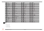
Table 15 PCI Express Signal Descriptions (General Purpose)
Signal
Pin # Description
I/O
PU/PD
Comment
P
PCIE_RX0-
B68
B69
PCI Express channel 0, Receive Input differential pair
I PCIE
P
PCIE_TX0-
A68
A69
PCI Express channel 0, Transmit Output differential pair
O PCIE
P
PCIE_RX1-
B64
B65
PCI Express channel 1, Receive Input differential pair
I PCIE
P
PCIE_TX1-
A64
A65
PCI Express channel 1, Transmit Output differential pair
O PCIE
P
PCIE_RX2-
B61
B62
PCI Express channel 2, Receive Input differential pair
I PCIE
P
PCIE_TX2-
A61
A62
PCI Express channel 2, Transmit Output differential pair
O PCIE
P
PCIE_RX3-
B58
B59
PCI Express channel 3, Receive Input differential pair
I PCIE
P
PCIE_TX3-
A58
A59
PCI Express channel 3, Transmit Output differential pair
O PCIE
P
PCIE_RX4-
B55
B56
PCI Express channel 4, Receive Input differential pair
I PCIE
P
PCIE_TX4-
A55
A56
PCI Express channel 4, Transmit Output differential pair
O PCIE
P
PCIE_RX5-
B52
B53
PCI Express channel 5, Receive Input differential pair
I PCIE
Shared with SATA port 1 and configurable via the BIOS setup
menu
P
PCIE_TX5-
A52
A53
PCI Express channel 5, Transmit Output differential pair
O PCIE
P
PCIE_RX6-
C19
C20
PCI Express channel 6, Receive Input differential pair
I PCIE
Shared with SATA port 0 and configurable via the BIOS setup
menu
P
PCIE_TX6-
D19
D20
PCI Express channel 6, Transmit Output differential pair
O PCIE
P
PCIE_RX7-
C22
C23
PCI Express channel 7, Receive Input differential pair
I PCIE
Shared with USB 3.2 Gen 1x2, port 3 and configurable via the
BIOS setup menu
P
PCIE_TX7-
D22
D23
PCI Express channel 7, Transmit Output differential pair
O PCIE
PCIE_
PCIE_CLK_REF-
A88
A89
PCI Express Reference Clock output for all PCI Express
and PCI Express Graphics Lanes
O PCIE
A PCI Express Gen2/3 compliant clock buffer chip must be
used on the carrier board if the design involves more than
one PCI Express device.
Note
The default BIOS setting for the shared ports is PCIe.


