


Classé CP-65 Software Upgrade
This document details the steps to upgrade your CP-65 Preamplifier from
software revision 65-102A47 to CS103B02.
This new release solves the random problem of the unit becoming unstable when
using the unity gain option.
Warning !
Before starting this procedure make sure the unit is shut off and unplugged from
the main A.C. line.
Section 1.0 Removing Main Unit Cover
To remove the cover of the CP-65 main unit simply remove the 8 medium sized
Philips screws and lift off the top cover.
Section 2.0 Replacing the Firmware IC
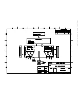
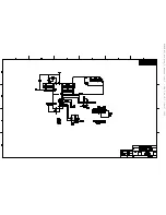
We have supplied 2 schematic diagrams, Figures 1 and 2, to help you locate the
integrated circuit (IC) that needs to be replaced. Figure 1 shows you the
complete layout of the main unit and a highlighted area in which the firmware
IC (U503) is located.
U503 is located in the center of figure 2 and above C340 and C317 when looking
at the unit with the front panel facing you. The IC is a dual inline package with 28
pins and is placed on the main board with the notch towards the rear panel.
Remove U503 with the supplied chip puller and replace it with the new IC
labeled CS103B02. Make sure you place the new IC with its’ notch facing the
rear of the unit.
Incorrect placement will of U503 will cause your CP-65 not to turn on.
Once you have replaced the IC you should power up the unit to ensure proper
placement and seating. When you have verified proper power up of the unit
you can then shut down the unit and replace the top cover. We have supplied
you with 8 new top cover screws to replace any damaged or marked during this
procedure.
Содержание CP-65
Страница 1: ...CP 65 Class PREAMPLIFIER SERVICE MANUAL v 1 0...
Страница 2: ...Index Mechanical Assembly 3 PC Boards 17 Testing Procedures 30 Diagrams 33...
Страница 3: ...CP 65 MECHANICAL ASSEMBLY...
Страница 5: ...FACE PLATE ASSEMBLY 1 2 3 4 5 L214XR01 S 6 Class 2 1 2 3 6 5 4 TOP VIEW SIDE VIEW 1 SIDE VIEW 2 CP 65...
Страница 6: ...CHASSIS REAR VIEW 1 2 3 4 5 6 7 8 Class 3 CP 65...
Страница 7: ...CHASSIS 1 PLA CAPFR1 2 HDW 8 FLAT WASHER 3 BZO 8 32x3 4 BHCS 4 Class 6 1 2 3 4 TOP VIEW CP 65...
Страница 9: ...CP 65 PC BOARDS...
Страница 10: ...MAINBOARD Class 10 CP 65 N A...
Страница 11: ...CP 65 TESTING PROCEDURES...
Страница 12: ...Class 14 START UP CP 65 N A...
Страница 13: ...CP 65 DIAGRAMS...
Страница 14: ...B2BXR00 Class 16 CP 65...
Страница 15: ...CP65_block sch 1 Thu Jun 20 11 11 21 2002...
Страница 16: ...B2B7XR03_amp sch 1 Thu Jun 20 11 00 56 2002...
Страница 17: ...B2B7XR03_amp sch 2 Thu Jun 20 11 01 28 2002...
Страница 18: ...B2B6XR00_IR_input sch 1 Thu Jun 20 10 59 40 2002...
Страница 19: ...B2B5XR01_Encoder sch 1 Thu Jun 20 10 59 01 2002...
Страница 20: ...B2B4XR01_display_5_button sch 2 Thu Jun 20 11 07 05 2002...
Страница 21: ...B2B4XR01_display_5_button sch 1 Thu Jun 20 11 08 57 2002...
Страница 22: ...B2b2XR00_line input2 sch 1 Thu Jun 20 10 56 01 2002...
Страница 23: ...B2B1XR02_mother_PCB_with cs3310 sch 1 Thu Jun 20 10 51 01 2002...
Страница 24: ...B2B1XR02_mother_PCB_with cs3310 sch 2 Thu Jun 20 10 51 38 2002...
Страница 25: ...B2B1XR02_mother_PCB_with cs3310 sch 3 Thu Jun 20 10 53 20 2002...
Страница 26: ...B2B1XR02_mother_PCB_with cs3310 sch 4 Thu Jun 20 10 54 28 2002...
Страница 27: ...B2B1XR02_mother_PCB_with cs3310 sch 5 Thu Jun 20 10 55 06 2002...
Страница 28: ...B2B8XR02_ext ps sch 1 Thu Jun 20 11 13 08 2002...
Страница 36: ......


