


VCC-G20X30B
Rev. 900-731-31-00
©2012 CIS Corporation. All rights reserved.
7
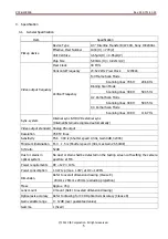
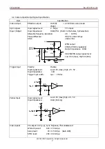
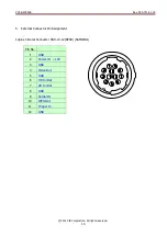
4.2. Camera Input/Output Signal Specification
Item Specification
Video output
Effective output:
1024(H)
×
768(V)
at full frame scan mode
Sync signals
Input /Output
Input signal level:
2
~
5Vp-p
TTL Input
Input impedance:
10k
Ω
/75
Ω
(Refer to the below, SW selection)
Allowable frequency deviation:
28
~
31MHz
Phase difference:
HD/VD: under 0±5
μ
s
Jitter: under
20ns
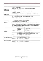
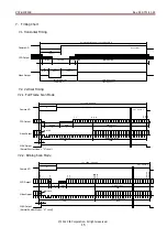
HD/VD
75
10k
SW
100
4.7k
33k
47pF
3.3V
IN/OUT
CMOS
5V
WEN output
CMOS (VHC04 equivalent)
Output impedance
100
Ω
HD/VD/WEN output signal level
Low 0.5V (max), High 4V (Min)
Trigger input
Polarity:
Positive
Input signal level:
Low 0.5V (max), High 2.5
~
5V
Input impedance:
1 k
Ω
Trigger input width:
4
μ
s
~
250ms
Partial Input
Input signal level:
Low 0.5V (max) High 2.5
~
5V
Input impedance:
10k
Ω
(Pull Up)
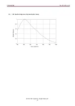
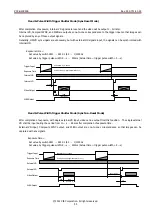
Video signal
VS output 1.0V (p-p), Sync. Negative, 75
Ω
unbalanced
White clip level:
820 ± 70 mVp-p
Setup level:
20 ± 15 mVp-p (Gain 0dB)
SYNC level:
290 ± 50 mVp-p


