6
DS241RD1C1
CRD4610-1
CrystalClear™ AC '97 Motherboard Reference Design
CIRRUS LOGIC ADVANCED PRODUCT DATABOOK
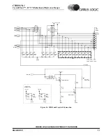
Figure
4
: Line Input
Two parallel 1
µ
F capacitors are used on the line in
circuit to decrease the low frequency corner since
this input is usually used for high signal quality in-
put. A 2
µ
F capacitor could be used, but 2
µ
F sur-
face mount capacitors are often not high quality
capacitors and can add distortion to audio signals.
Figure
6
: Headphone or Headset
A resistor population option is included to choose
between a headphone or headset connection. The
headset connection incorporates the right head-
phone and MIC2 on one external jack.
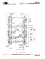
Figure
14
: MIDI and Joystick Connection
A buffer driver circuit is used on the MIDI output
pin to provide the necessary drive for MIDI devices
connected through a long cable. This circuit can be
removed, and R28 populated to bypass the buffer
driver circuit if it is unnecessary.
Figure
15
: PCI Bus Connection
The PCI 2.1 specification requires that each unused
+3.3 V power pin should be connected with an av-
erage of 0.01
µ
F capacitor [2]. Two 0.1
µ
F capaci-
tors in parallel provide the required capacitance for
the power pins.
EMC Components
A number of capacitors and inductors are included
to help the board meet EMC compliance tests, such
as FCC Part 15. These components are outlined in
the schematic. They may or may not be needed in a
particular design, so the footprints are added in
case they are necessary. EMC testing should show
where problem areas exist, and components can be
added to those areas. EMC components can also be
removed in areas that do not show problems.
GROUNDING AND LAYOUT
The routing of the CRD4610-1 provides a good ex-
ample of how a PCI add-in card should look. PCI-
bus based add-in cards have explicit requirements
on trace lengths that are not imposed on mother-
board designs. These trace length limits for add-in
cards are as follows:
•
Maximum trace length for 32-bit signals on 32-
bit and 64-bit cards is 1.5 inches.
•
Maximum trace lengths for signals on the 64-
bit extension are 2 inches.
•
Trace length for the PCI CLK signal is 2.5 inch-
es ± 0.1 inch.
•
The PCI CLK signal must drive only one load.
Please refer to the PCI 2.1 Specification Section
4.3.6 for information on routing PCI bus signals on
a motherboard [2].
Partitioned Voltage and Ground Planes
The CRD4610-1 is partitioned into a digital and an-
alog section. Correspondingly, the voltage and
ground planes are partitioned to keep digital and
analog ground currents from crossing. Ground cur-
rents from digital signals are inherently noisy with
respect to analog signals and should be isolated
from the audio section. The first rule in laying out
mixed signal PCBs is to keep all digital signals
over the digital ground plane and all analog signals
over the analog ground plane. When digital and an-
alog signals cross planes, they introduce noise into
the audio section reducing performance.
The pinout of the CS4297 allows the ground split to
completely separate digital signals on one side and
analog signals on the other. This split is located
very close to the CS4297 so analog and digital
ground return currents originating from the
CS4297 may flow through their respective ground
planes. A bridge is made across the split to main-
tain the proper reference potential for each ground
plane.
Another small partition in the digital ground plane
is for the crystal oscillator. The data converters in
the CS4297 are highly susceptible to noise on the
Содержание CRD4610-1
Страница 30: ......


