background image

DS241RD1C1

5

CRD4610-1

CrystalClear™ AC '97 Motherboard Reference Design

CIRRUS LOGIC ADVANCED PRODUCT DATABOOK

Other Reference Card Features

Other reference card features that are not associat-
ed with the other sections are the external volume
control buttons, the joystick/MIDI connection, and
the power regulators.

Volume Control Buttons

The volume control buttons are connected to the
CS4610 and act as a master volume control. The
four-pin header can be populated to provide a cable
connection for volume control buttons that can be
placed elsewhere in the system. There is a volume
up button and a volume down button. Pressing both
buttons at the same time enables the mute/unm-
mute function.

Joystick/MIDI connection

The DB-15 connector allows a joystick or an exter-
nal MIDI device to be connected to the CS4610. In
the AC’ 97 configuration, the CS4610 handles the
joystick operation. The external connection can
also take MIDI data from an external source to the
CS4610. A buffer circuit allows the MIDIOUT pin
of the CS4610 to drive an external MIDI input.

Power Regulators

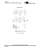
There are two power regulators on the board. One
is a Linear Technologies LT117CST-3.3 voltage
regulator that derives the +3.3 V supply for the
CS4610 and the CS4297 from the +5 V on the PCI
bus. This regulator is unnecessary on mother
boards with a +3.3 V supply. The regulator was
used in this reference design because the +3.3 V
PCI bus power pins are not guaranteed to be on the
PCI bus connector.  The card is also designed to be
used in a 5 V PCI Connector [2]. 

A Motorola MC78M05CDT regulates the PCI
+12 V supply down to provide a clean +5 V analog
supply for the operational amplifiers and the
CS4297. A power regulator is recommended for
the analog voltage supply to provide good audio
signal quality. The MC78M05CDT regulator can

provide up to 500 mA of current with adequate
heat-sinking, which is enough power for the
CS4297 and the three audio op-amps. The
MC78L05 power regulators do not provide enough
current to power the same devices, and are not rec-
ommended for use with the CS4297.

SCHEMATIC DESCRIPTION

Figures 1 through 8 show the schematics for the
CRD4610-1 card. This section will describe partic-
ular pages of the schematic that need to be dis-
cussed.

Figure 

7

 : CD Audio Input

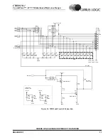
C5 and C6 are used in parallel to make a 2

µ

F ca-

pacitor on the CD Common line because the input
impedance on that line is half of what is on the CD
In Right and CD In Left. A 2

µ

F capacitor could be

used, but many of the 2

µ

F capacitors tested have

shown distortion problems.

Figure 

3

 : CS4297

A 10

µ

F electrolytic capacitor should be added

next to pins 25 and 26 if the capacitor connected to
the output of the power regulator is located far
away from the CS4297. For the best audio perfor-
mance, the analog voltage regulator should be lo-
cated near the CS4297. R1 and R2 are termination
resistors in the serial AC link between the CS4297
and the CS4610. NPO-type capacitors should be
used on all loading capacitors of audio signals to
ensure minimal added distortion.

Figure 

2

 : CS4610

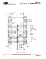
The 0.1

µ

F capacitors connected to the power pins

of the CS4610 should be as close as possible to the
chip. The inductor L6 is used to filter the power
supply for the internal PLL circuit. R7 can be re-
moved from a production design, and pin 51 can be
connected directly to digital ground. R3 and R4 are
termination resistors in the serial AC link between
the CS4297 and the CS4610.

Содержание CRD4610-1

Страница 1: ...and PC 98 both required and advanced audio performance requirements DESCRIPTION The CRD4610 1 showcases Cirrus Logic s Cystal Audio AC 97 motherboard solution using the CS4610 SoundFusion Audio Accelerator and the CS4297 SoundFusion Audio Codec 97 This de sign illustrates a single sided motherboard implementation on a PCI adapter card Using the Mic In Line Out and Line In analog connectors only th...

Страница 2: ...layout The reference design card is sectioned into three main parts the CS4610 PCI Audio Accelerator section the CS4297 Audio Codec 97 section and the Optional Extended Analog I O section CS4610 PCI Audio Accelerator Section The area around the CS4610 includes the required bypass capacitors PLL power supply filter compo nents an EEPROM the components for the joy stick connection and a buffer circu...

Страница 3: ... the microphone 2 input on the tip connection of the external jack and the right headphone channel on the ring connection of the external jack The Modem Audio CD ROM Video In Aux in and Spk In headers are also part of the Extended Analog I O section Each header has a few resistor packs and capacitors associated with it The header and its associated components may or may not be necessary depending ...

Страница 4: ... jack Ring connection Mono input Maximum input level 1 Vrms Tip connection Mono output Maximum output level 0 7 Vrms Headphone Out or Headset An external 1 8 jack is provided for a headphone or headset connection The card comes configured for headphone operation with the selection being made by a 0 Ω resistor population option The headphone option is selected by populating R24 and R26 and not popu...

Страница 5: ...5 V analog supply for the operational amplifiers and the CS4297 A power regulator is recommended for the analog voltage supply to provide good audio signal quality The MC78M05CDT regulator can provide up to 500 mA of current with adequate heat sinking which is enough power for the CS4297 and the three audio op amps The MC78L05 power regulators do not provide enough current to power the same device...

Страница 6: ...LAYOUT The routing of the CRD4610 1 provides a good ex ample of how a PCI add in card should look PCI bus based add in cards have explicit requirements on trace lengths that are not imposed on mother board designs These trace length limits for add in cards are as follows Maximum trace length for 32 bit signals on 32 bit and 64 bit cards is 1 5 inches Maximum trace lengths for signals on the 64 bit...

Страница 7: ...developer intel com pc supp platform ac97 2 PCI Special Interest Group PCI Local Bus Specification Revision 2 1 June 1 1995 http www pcisig com 3 Cirrus Logic CS4610 SoundFusion PCI Audio Accelerator Data Sheet http www cirrus com products overviews cs4610 html 4 Cirrus Logic CS4297 SoundFusion Audio Co dec 97 Data Sheet http www cirrus com products overviews cs4297 html 5 Steve Harris Clif Sanche...

Страница 8: ...EF MIC1 MIC2_IN VREF MIC2 HP_OUT_R HP_OUT_L PC_BEEP PC_BEEP PHONE_IN MONO_OUT PHONE_IN VIDEO_IN VIDEO_R VIDEO_L HEADPHONE_OUT VREF ALT_LINE_OUTR ALT_LINE_OUTL HP_OUT_L HP_OUT_R C BE2 STOP SERR FRAME TRDY AD 31 0 IDSEL PERR PAR IRDY C BE0 DEVSEL C BE1 GNT CLK RST INTA REQ C BE3 MIDIIN MIDIOUT JBB2 JBB1 JBCY JBCX JAB2 JAB1 JACY JACX VREF LINE_OUTL LINE_OUTR LINE_INR LINE_INL VREF MIC1 PHONE_IN MONO_...

Страница 9: ... 28 AD14 29 AD13 32 AD12 33 AD11 34 AD10 35 AD09 36 AD08 37 CBEO 38 AD07 41 AD06 42 AD05 43 AD04 44 AD03 45 AD02 46 AD01 47 AD00 48 JBB2 MCLK 59 JAB2 SDO3 57 MIDIIN 60 MIDIOUT 63 SDIN2 GPIO 66 VOLUP XTALI 70 VOLDN XTALO 71 EECLK GPOUT 79 EEDAT GPIO2 80 TEST 51 INTA 81 RST 82 PCICLK 83 PCI_GNT 84 PCI_REQ 85 AD24 97 AD25 96 AD27 92 AD28 91 AD29 90 AD30 89 AD31 88 AD26 95 CRYVDD 69 CVDD0 19 CVDD1 12 ...

Страница 10: ... 390pF NPO C143 1 0uF Y5V C18 680pF NPO C19 680pF NPO C17 680pF NPO C15 680pF NPO U CS4297 KQ LINE_OUT_R 36 MONO_OUT 37 AVdd2 38 ALT_LINE_OUT_L 39 NC7 44 ALT_LINE_OUT_R 41 AVss2 42 NC6 43 NC5 40 NC4 34 NC3 33 NC2 32 NC1 31 DVdd1 1 XTL_IN 2 XTL_OUT 3 DVss1 4 SDATA_OUT 5 BIT_CLK 6 DVss2 7 SDATA_IN 8 SYNC 10 DVdd2 9 RESET 11 PC_BEEP 12 PHONE 13 AUX_L 14 AUX_R 15 VIDEO_L 16 VIDEO_R 17 CD_L 18 CD_GND 1...

Страница 11: ...0uF Y5V C142 1 0uF Y5V RP18 6 8k 4 1 2 3 RP19 6 8k 4 1 2 3 LINE_INR LINE_INL EMC Figure 4 Line Input AGND 5VA AGND 5VA AGND AGND CGND 5VA AGND Connect CGND to AGND at the jack U5A MC33078D 3 2 1 8 4 U5B MC33078D 5 6 7 8 4 C77 0 33uF X7R C76 3 3uF ELEC R16 2 2k R15 47k R12 47k R17 6 8k C78 100pF NPO C79 100pF NPO C74 220pF NPO J7 PHONO 1 8 4 3 5 2 1 C73 100pF NPO C75 0 33uF X7R C71 0 1uF Y5V R14 47...

Страница 12: ...A MC33078D 3 2 1 8 4 C85 0 33uF X7R C84 0 33uF X7R C88 3 3uF ELEC R22 47k R19 47k R23 6 8k U6B MC33078D 5 6 7 8 4 C83 220pF NPO J8 PHONO 1 8 4 3 5 2 1 C82 100pF NPO R26 0 R24 0 R25 0 R18 2 2k C80 0 1uF Y5V C86 390pF NPO C87 390pF NPO R21 47 VREF MIC2 HP_OUT_L HP_OUT_R L AND R HEADPHONES POPULATE R26 AND R24 DO NOT POPULATE R25 R HEADPHONE AND MIC2 POPULATE R25 DO NOT POPULATE R26 AND R24 EMC Figur...

Страница 13: ... 0uF Y5V L3 31 100MHz L4 31 100MHz L5 31 100MHz RP3 3 4k 4 1 2 3 C6 1 0uF Y5V J2 B4B PH K 1 2 3 4 RP16 6 8k 4 1 2 3 RP17 6 8k 4 1 2 3 CD_INR CD_INL CD_COM EML Figure 7 CD Audio Input AGND AGND VIDEO IN L GND GND R C134 1 0uF Y5V C135 1 0uF Y5V L8 31 100MHz L9 31 100MHz J12 4X1HDR 1 2 3 4 RP20 6 8k 4 1 2 3 RP21 6 8k 4 1 2 3 VIDEO_R VIDEO_L EMC Figure 8 Video Audio Input ...

Страница 14: ...1 4X1HDR 1 2 3 4 RP14 6 8k 4 1 2 3 RP15 6 8k 4 1 2 3 AUX_R AUX_L EML Figure 9 Aux Input AGND AGND AGND CGND AGND EXTERNAL MODEM MONO OUT PHONE IN GND INTERNAL MODEM CONNECTION GND Connect CGND to AGND at the jack C125 1 0uF Y5V R35 47k R36 47k J11 PHONO 1 8 4 3 5 2 1 C126 100pF NPO C127 100pF NPO R34 20K C124 1 0uF Y5V J13 4X1HDR 1 2 3 4 MONO_OUT PHONE_IN EMC Figure 10 MODEM Audio Connection ...

Страница 15: ... than a transistor PC Speaker IN J10 HDR2X1 1 2 C123 2700pF X7R R32 4 7k 1 2 R33 47k L7 31 100MHz C122 0 1uF Y5V PC_BEEP EMC Figure 11 PC Speaker Input AGND CGND AGND AGND INTERNAL LINE OUT L GND GND R Connect CGND to AGND at the jack J5 PHONO 1 8 4 3 5 2 1 J6 4X1HDR 1 2 3 4 C67 10uF ELEC C68 10uF ELEC C69 390pF NPO C70 390pF NPO R42 1 MEG R41 1 MEG LINE_OUTR LINE_OUTL EMC Figure 12 Line Output ...

Страница 16: ...VA 5VA AGND 5VA AGND Place close as possible to U4 1 4 WATT 1 4 WATT U4A TDA1308 3 2 1 8 4 U4B TDA1308 5 6 7 8 4 RP6 27k 4 1 2 3 RP7 39k 4 1 2 3 C59 22pF NPO C62 22pF NPO R8 10 R9 10 RP8 47K 4 1 2 3 C58 0 1uF Y5V C60 220uF ELEC C61 220uF ELEC VREF ALT_LINE_OUTR ALT_LINE_OUTL HP_OUT_L HP_OUT_R Figure 13 Headphone Amplifier ...

Страница 17: ... 4 7 6 5 C96 1000pF X7R 1 2 C95 1000pF X7R 1 2 C93 1000pF X7R 1 2 C94 1000pF X7R 1 2 C89 5600pF X7R C90 5600pF X7R C91 5600pF X7R C92 5600pF X7R R27 47k Q1 MMBT2907ALT1 1 3 2 Q2 MMBT3904LT1 1 3 2 RP13 39k 4 1 2 3 R30 10K R31 20K R28 0 R29 5 1K C108 1000pF X7R 1 2 C112 1000pF X7R 1 2 C97 100pF NPO C98 100pF NPO C99 100pF NPO C100 100pF NPO C101 100pF NPO C102 100pF NPO C103 100pF NPO C104 100pF NPO...

Страница 18: ...V3 33 FRAME 34 GND6 35 TRDY 36 GND7 37 STOP 38 3 3V4 39 SDONE 40 SBO 41 GND8 42 PAR 43 AD15 44 3 3V5 45 AD13 46 AD11 47 GND9 48 AD9 49 KEY1 50 KEY2 51 C BE0 52 3 3V6 53 AD6 54 AD4 55 GND10 56 AD2 57 AD0 58 5V5 59 REQ64 60 5V6 61 5V7 62 P2 PCI_BUS_5V_B Side B 12V 1 TCK 2 GND11 3 TDO 4 5V8 5 5V9 6 INTB 7 INTD 8 PRSNT1 9 RSVD5 10 PRSNT2 11 GND12 12 GND13 13 RSVD6 14 GND14 15 CLK 16 GND15 17 REQ 18 5V...

Страница 19: ... Connect AGND to DGND with a 50 mil trace near the 4297 Connect CGND to DGND with a 50 mil trace near the finger edge of the board F1 FUSE PTC C133 0 01UF X7R 1 2 C132 0 1uF Y5V C128 10uF ELEC C130 10uF ELEC L10 31 100MHz C140 0 1uF Y5V H1 HOLE 1 C129 10uF ELEC U9 MC78M05CDT OUT 3 GND 2 IN 1 C131 100uF ELEC U10 LT1117CST 3 3 OUT 2 GND 1 IN 3 TAB OUT 4 EMC Figure 16 Power Supplies ...

Страница 20: ...20 DS241RD1C1 CRD4610 1 CrystalClear AC 97 Motherboard Reference Design CIRRUS LOGIC ADVANCED PRODUCT DATABOOK Figure 17 Top Side Silk Screen ...

Страница 21: ...DS241RD1C1 21 CRD4610 1 CrystalClear AC 97 Motherboard Reference Design CIRRUS LOGIC ADVANCED PRODUCT DATABOOK Figure 18 Top Layer Route ...

Страница 22: ...22 DS241RD1C1 CRD4610 1 CrystalClear AC 97 Motherboard Reference Design CIRRUS LOGIC ADVANCED PRODUCT DATABOOK Figure 19 Gnd Layer ...

Страница 23: ...DS241RD1C1 23 CRD4610 1 CrystalClear AC 97 Motherboard Reference Design CIRRUS LOGIC ADVANCED PRODUCT DATABOOK Figure 20 VCC Layer ...

Страница 24: ...24 DS241RD1C1 CRD4610 1 CrystalClear AC 97 Motherboard Reference Design CIRRUS LOGIC ADVANCED PRODUCT DATABOOK Figure 21 Bottom Side Route ...

Страница 25: ...DS241RD1C1 25 CRD4610 1 CrystalClear AC 97 Motherboard Reference Design CIRRUS LOGIC ADVANCED PRODUCT DATABOOK Figure 22 Assembly Drawing ...

Страница 26: ...26 DS241RD1C1 CRD4610 1 CrystalClear AC 97 Motherboard Reference Design CIRRUS LOGIC ADVANCED PRODUCT DATABOOK Figure 23 Drill Drawing and Manufacturing Instructions ...

Страница 27: ...KCV CAP 22pF 0603 5 50V NPO 5 5 C15 C16 C17 C18 C19 680pF PANASONIC ECU V1H681JCX CAP 680pF 0805 5 50V NPO 6 6 C24 C25 C69 C70 C86 C87 390pF PANASONIC ECU V1H391KCV CAP 390pF 0603 10 50V NPO 7 20 C36 C37 C65 C66 C73 C78 C79 C82 C97 C98 C99 C100 C101 C102 C 103 C104 C10 5 C106 C126 C127 100pF PANASONIC ECU V1H101KCV CAP 22pF 0603 5 50V X7R 8 3 C38 C114 C13 3 0 01UF PANASONIC ECU V1H103KBV CAP 0 01F...

Страница 28: ...1 RP5 100 PANASONIC EXB V4V101JV RES ARRAY 2 ISOLATED 100 1 16W 5 0 6mm SMT 33 1 RP6 27k PANASONIC EXB V4V273JV RES ARRAY 2 ISOLATED 27k 1 16W 5 0 6mm SMT 34 2 RP7 RP13 39k PANASONIC EXB V4V393JV RES ARRAY 2 ISOLATED 39k 1 16W 5 0 6mm SMT 35 1 RP8 47K PANASONIC EXB V4V473JV RES ARRAY 2 ISOLATED 47K 1 16W 5 0 6mm SMT 36 1 RP11 2 2k PANASONIC EXB V8V222JV RES ARRAY 4 ISOLATED 2 2K 1 16W 5 0 6mm SMT ...

Страница 29: ...R 53 1 U3 X24C04 ATMEL AT24C04N 10SC IC 24C04 512X8BIT SO SOIC8 EEPR OM 54 1 U4 TDA1308 PHILIPS TDA1308S8 IC 1308 SO SOIC8 LOW NOISE HEADPHONE AMP 55 2 U5 U6 MC33078D MOTO MC33078D IC 33078 SO SOIC8 DUAL OP AMP 56 1 U10 LT1117CST 3 3 LINEAR TECHNOLO GY LT1117CST 3 3 3 3V REGULATOR SOT_223 0 2 800mA 57 1 U9 MC78M05CDT MOTOROLA MC78M05CDT 5V REGULATOR DPAK 2 500MA 58 1 Y1 24 576 MHz EPSON CA 301_24 ...

Страница 30: ......
Отзывы: