background image

4.  Start AVR Studio and establish a new project only one time. See section on how to 

start a new debugging project  

5.  Load the select Coff file, built using the make file option extcoff 

6.  Start debugging   

Note: 

When using the JTAG ICE programmer the boot vector fuse must be disabled. 


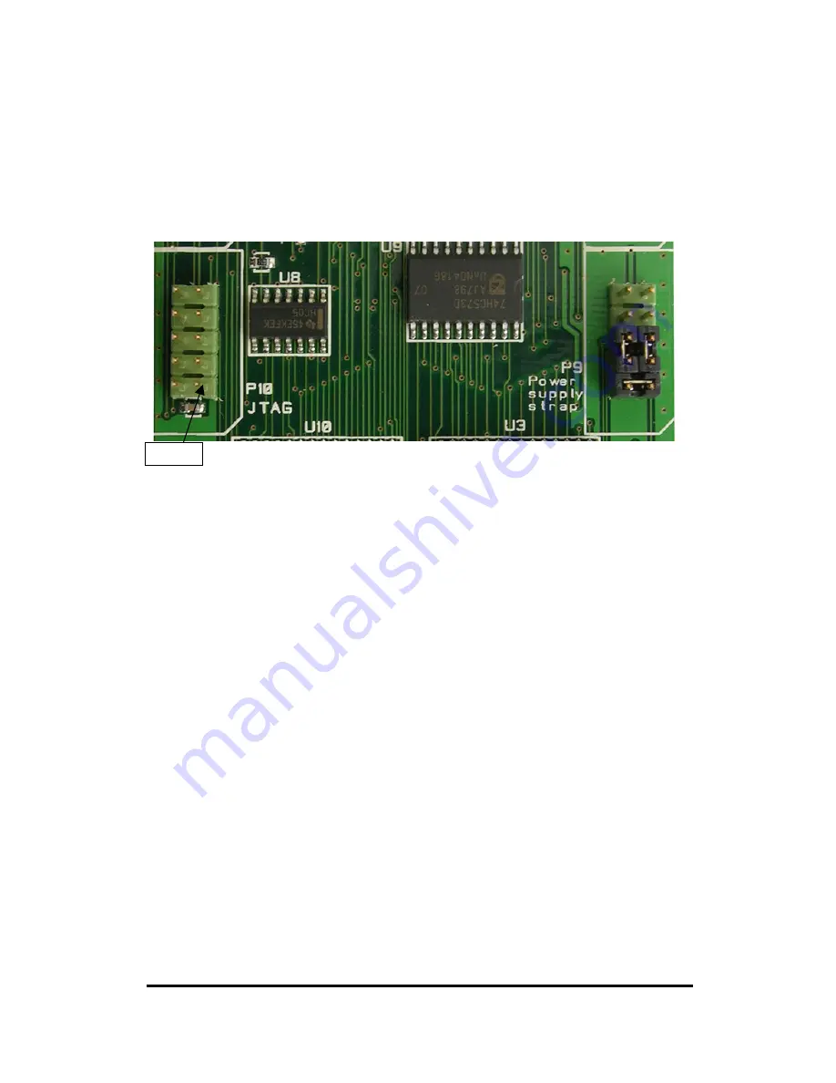
Pin 1 

Figure 21: JTAG ICE connector P10 on CC2420DB 

Saving the IEEE Address of the CC2420DB  

Before any debugging is preformed on the CC2420DB, the content of the Atmega128L 
EEPROM memory must be read and saved to a disk file on the development computer.  This 
will allow the IEEE address to be restored if the EEPROM gets erased or corrupted. The AVR 
Studio program in conjunction with the JTAG ICE or AVR ISP is applied to upload the 
EEPROM data from the Atmega128L microcontroller and recorded to the disk file specified by 
the user. 

When a project is first created in AVR Studio, the EEPROM will be erased when the .

cof

 file 

is downloaded to the CC2420DB. Due to this, it is important to save the EEPROM content to 
a disk file before creating the new project. The following procedure can be applied to save 
EEPROM data initially or at any desired time: 

• 

With power removed from the CC2420DB, connect the JTAG ICE, JTAG ICE mkII or 
AVR ISP to the their respective connectors on the CC2420DB. Make sure the JTAG 
cable is oriented correctly. Please refer to figure 21 to see where pin 1 is located. 


Chipcon AS       

 SmartRF

®

 CC2420DBK Demonstration Board Kit User Manual 

 (rev. 1.3) 2004-11-03 Page 34/ 52  

Содержание SmartRF CC2420DBK

Страница 1: ...User Manual Rev 1 3 SmartRF CC2420DBK Demonstration Board Kit Chipcon AS Gaustadalléen 21 NO 0349 Oslo Norway Tel 47 22 95 85 45 fax 47 22 95 85 46 E mail support chipcon com ...

Страница 2: ...N USING AVR STUDIO 4 30 PREPROGRAMMED 64 BIT IEEE ADDRESS 30 PREPROGRAMMED FUSES 31 PREPROGRAMMED LOCK BITS 33 JTAG ICE OR JTAG ICE MKII 33 SAVING THE IEEE ADDRESS OF THE CC2420DB 34 RESTORING THE IEEE ADDRESS OF THE CC2420DB 36 A NEW DEBUGGING PROJECT WITH CC2420DB 38 BOOTLOADER 43 INTRODUCTION TO EXAMPLES PROVIDED WITH CC2420DB 45 LIBRARIES AND EXAMPLES 45 HARDWARE DEFINITION FILES 45 HARDWARE A...

Страница 3: ...al user application interface The demonstration board is also furnished with connectors where all of the internal signals on the PCB are available This User Manual describes how to use the CC2420DBK Demonstration Board Kit Atmel s AVR Studio and associated software is used to program and debug software Please see the reference section of this document for links to Atmel s documentation on how to u...

Страница 4: ...4 11 03 Page 4 52 Figure 1 CC2420DB overview RF Section The CC2420DB RF section includes all the necessary components for correct operation The CC2420 is connected to a 16 MHz crystal A small 2 4 GHz PCB antenna is also included RF test and measurement equipment can be connected to the SMA on the PCB by swapping Temp sensor External RAM 1 x 32 kB JTAG connector MCU section CC2420 RF section PCB an...

Страница 5: ... H will in general decrease the antenna bandwidth Please see Figure 2 for the antenna dimensions Figure 2 Antenna dimensions The height of the antenna is defined as the distance from the ground plane to the parallel section and the length is from the end of the antenna parallel section to the feed point Length L 26 19 mm 9 19 mm 1 22 mm x 17 61 mm Height H 6 17 mm 0 97 mm 1 19 mm x 6 55 mm Quarter...

Страница 6: ...se note that these range tests were performed with a simple packet protocol no link margin no robust protocol close to the sensitivity limit of CC2420 and no retransmission CC2420DB 0 degr Top view Antenna Figure 3 Radiated pattern horizontal mounting Figure 3 depicts the antenna pattern while the CC2420DB is mounted horizontally with the antennas parallel section aligned to the 0 degree direction...

Страница 7: ...I O pins of the CC2420 The internal regulator of CC2420 is used to generate the 1 8 voltage supply applied for powering of the CC2420 core A diode prevents permanent damage if wrong polarity is applied to the board There are two power connectors a 2 5mm DC jack type connector allows you to connect an unregulated battery eliminator easily the positive supply is on the center pin and a connector for...

Страница 8: ... to add a daughter board with additional circuitry using these connectors External RAM The lower 4 Kbytes of the external RAM is overlaid by the Atmega128L internal register and RAM CC2420DB includes this memory because it can be used for debugging purposes to buffer and store data if desired The 32 kB RAM size is not a requirement nor necessary for a low cost a Full Functional Device FFD or Reduc...

Страница 9: ...ed by the crystal tolerance and the CC2420 temperature range Jumper settings for demonstration board control The CC2420DB demonstration board has three default jumper settings for proper operation Figure 5 depicts the placement of the three jumpers J1 J2 and J3 They are mounted on connector P9 Please see CC2420DB schematics page 1 for more details Jumper Purpose Comments J1 To apply power of 3 3 v...

Страница 10: ... RS 232 driver U101 the jumper J3 can be moved Step By Step procedure 1 Move RS 232 jumper J3 from P9 to P3 between pin 3 and 4 2 It will share the same port pin PE4 as the yellow LED so when RS 232 is on the LED will be set Chipcon AS SmartRF CC2420DBK Demonstration Board Kit User Manual rev 1 3 2004 11 03 Page 10 52 ...

Страница 11: ...f the CC2420DB for a specific IEEE 802 15 4 devices the default jumper J3 can be moved to enable software control of the RS 232 driver The external RAM will always draw 2mA in any power down mode since its power supply cannot be disabled Hence if the external RAM U3 is removed the current consumption will decrease with 2mA The jumper J2 is controlling the power for the potentiometer RT1 and temper...

Страница 12: ...erface SI CC2420 P4 pin 8 13 PB3 MISO SPI Interface SO CC2420 P4 pin 6 14 PB4 OC0 Orange LED P3 pin 18 15 PB5 OC1A VREG_EN Enable volt regulator on CC2420 P4 pin 10 16 PB6 OC1B RESETn CC2420 P4 pin 16 17 PB7 OC2 OC1C Green LED P3 pin 16 18 PG3 TOSC2 External 32 kHz crystal General purpose I O P3 pin 7 19 PG4 TOSC1 External 32 kHz crystal General purpose I O P3 pin 9 20 RESET Reset Switch S2 ISP JT...

Страница 13: ... AD7 RAM address Data N A 45 PA6 AD6 RAM address Data N A 46 PA5 AD5 RAM address Data N A 47 PA4 AD4 RAM address Data N A 48 PA3 AD3 RAM address Data N A 49 PA2 AD2 RAM address Data N A 50 PA1 AD1 RAM address Data N A 51 PA0 AD0 RAM address Data N A 52 VCC Supply power N A 53 GND Ground N A 54 PF7 ADC7 TDI JTAG interface P10 pin 9 55 PF6 ADC6 TDO JTAG interface P10 pin 3 56 PF5 ADC5 TMS JTAG inter...

Страница 14: ...SP MOSI Joystick up 02 PE0 7 PG3 External 32 kHz crystal General purpose I O 18 PG3 8 PE1 ISP MISO Joystick right 03 PE1 9 PG4 External 32 kHz crystal General purpose I O 19 PG4 10 PE5 Push button S2 07 PE5 11 PE3 Red LED N A 12 PE6 Joystick interrupt 08 PE6 13 RTS RS 232 handshaking 30 PD5 14 PE7 External interrupt General purpose I O 09 PE7 15 RXD1 RS 232 data from PC 27 PD2 16 PB7 Green LED 17 ...

Страница 15: ...6 SO CC2420 SPI out 34 SO 13 7 PF2 Joystick N A 59 8 SI CC2420 SPI in 33 SI 12 9 PF3 Temperature sensor N A 58 10 VREG_EN CC2420 voltage regulator enable 41 VREG_EN 15 11 PF0 Potentiometer N A 61 12 FIFO CC2420 FIFO 30 FIFO 26 13 CSn CC2420 SPI chip select 31 CSn 10 14 FIFOP CC2420 FIFOP 29 FIFOP 25 15 3 3V 3 3V Regulated supply N A N A 16 RESETn CC2420 Reset 21 RESETn 16 17 N C N A N A N A 18 CCA...

Страница 16: ...sed is standard FR 4 board material The PCB is 1 0mm thick with layer 1 on the topside layers 2 and 3 are internal layers and layer 4 is on the bottom side Layers 1 and 4 are used for routing while layer 2 is a ground plane and layer 3 is used for power routing All areas in the RF section that are not utilized for routing are filled with copper connected to ground to provide RF shielding The groun...

Страница 17: ...Layer 1 Layer 2 Layer 3 Layer 4 Figure 9 CC2420DB PCB layout Chipcon AS SmartRF CC2420DBK Demonstration Board Kit User Manual rev 1 3 2004 11 03 Page 17 52 ...

Страница 18: ...Top Assembly Bottom Assembly Figure 10 CC2420DB PCB layout silkscreen Chipcon AS SmartRF CC2420DBK Demonstration Board Kit User Manual rev 1 3 2004 11 03 Page 18 52 ...

Страница 19: ...Schematic Figure 11 CC2420DB schematic page 1 Chipcon AS SmartRF CC2420DBK Demonstration Board Kit User Manual rev 1 3 2004 11 03 Page 19 52 ...

Страница 20: ...Figure 12 CC2420DB schematic page 2 Chipcon AS SmartRF CC2420DBK Demonstration Board Kit User Manual rev 1 3 2004 11 03 Page 20 52 ...

Страница 21: ...Figure 13 CC2420DB schematic page 3 Chipcon AS SmartRF CC2420DBK Demonstration Board Kit User Manual rev 1 3 2004 11 03 Page 21 52 ...

Страница 22: ...Figure 14 CC2420DB schematic page 4 Chipcon AS SmartRF CC2420DBK Demonstration Board Kit User Manual rev 1 3 2004 11 03 Page 22 52 ...

Страница 23: ...Figure 15 CC2420DB schematic page 5 Chipcon AS SmartRF CC2420DBK Demonstration Board Kit User Manual rev 1 3 2004 11 03 Page 23 52 ...

Страница 24: ...Figure 16 CC2420DB schematic page 6 Chipcon AS SmartRF CC2420DBK Demonstration Board Kit User Manual rev 1 3 2004 11 03 Page 24 52 ...

Страница 25: ..._0402_X5R_K_10 C261 Capacitor 0402 100nF 10 C_100N_0402_X5R_K_10 C351 Capacitor 0402 100nF 10 C_100N_0402_X5R_K_10 C371 Capacitor 0402 68pF 5 C_68P_0402_NP0_J_50 C381 Capacitor 0402 27pF 5 C_27P_0402_NP0_J_50 C391 Capacitor 0402 27pF 5 C_27P_0402_NP0_J_50 C421 Capacitor 0805 10uF 15 C_10U_0805_X5R_L_25 C431 Capacitor 0805 10uF 15 C_10U_0805_X5R_L_25 C441 Capacitor 0402 68pF 5 C_68P_0402_NP0_J_50 C...

Страница 26: ...n It is possible to choose a larger crystal package to save cost The crystal should have an ESR of 60 Ω or less Bill of materials CC2420DB MCU section Reference Description Value Part C303 Capacitor 0603 100nF 10 C_100N_0603_X7R_K_50 C304 Capacitor 0603 100nF 10 C_100N_0603_X7R_K_50 C305 Capacitor 0603 100nF 10 C_100N_0603_X7R_K_50 C306 Capacitor 0603 100nF 10 C_100N_0603_X7R_K_50 C307 Capacitor 0...

Страница 27: ...7K_0603_G R308 Resistor 0603 47kΩ 2 R_47K_0603_G R309 Resistor 0603 47kΩ 2 R_47K_0603_G R310 Resistor 0603 47kΩ 2 R_47K_0603_G R311 Resistor 0603 47kΩ 2 R_47K_0603_G R312 Resistor 0603 0Ω R_0_0603 R313 Resistor 0603 47kΩ 2 R_47K_0603_G R314 Resistor 0603 R_10K_0603_G RT1 Trimming pot 10K knob R_0 10K_TRIM S1 Push button SMD PUSH_BUTTON S2 Push button SMD PUSH_BUTTON U1 Atmel microcontroller MLF64 ...

Страница 28: ...iode 2A 20BQ030 P7 9V battery connector positive CONN_9V_POS P8 9V battery connector negative CONN_9V_NEG U4 3 3 V low drop regulator 500 m MIC5209 3 3BS Bill of materials CC2420DB RS 232 section Reference Description Value Part C501 Capacitor 0603 100nF 10 C_100N_0603_X7R_K_50 C502 Capacitor 0603 100nF 10 C_100N_0603_X7R_K_50 C503 Capacitor 0603 100nF 10 C_100N_0603_X7R_K_50 C504 Capacitor 0603 3...

Страница 29: ...00nF 10 C_100N_0603_X7R_K_50 R601 Resistor 0603 10kΩ 2 R_10K_0603_G R602 Resistor 0603 10kΩ 2 R_10K_0603_G R603 Resistor 0603 10kΩ 2 R_10K_0603_G R604 Resistor 0603 10kΩ 2 R_10K_0603_G R605 Resistor 0603 10kΩ 2 R_10K_0603_G R606 Resistor 0603 10kΩ 2 R_10K_0603_G R607 Resistor 0603 10kΩ 2 R_10K_0603_G R608 Resistor 0603 10kΩ 2 R_10K_0603_G R609 Resistor 0603 10kΩ 2 R_10K_0603_G U10 32kB SRAM IDT71V...

Страница 30: ...st the Baud rate error for different crystal frequencies and Baud rates CC2420 Software Download and Evaluation Using AVR Studio 4 Use a serial cable to connect the serial interface of the CC2420DB to the serial port of a PC running AVR Studio Our SmartRF Studio cannot communicate with the CC2420DB but can be used to find register values for the CC2420 Power supply 220V PC running AVRStudio Serial...

Страница 31: ...ram downloading SPI enabled 4 Preserve EEPROM memory through the Chip Erase Cycle 5 Boot Flash section size 512 Boot start address 6 Boot vector enabled default address 0000 7 Brown out detection level at VCC 2 7 V 8 Brown out detection enabled 9 Ext Crystal Resonator High Freq Start Up time 16CK 64 ms CKSEL 1111 SUT 11 Note When using the JTAG ICE mkII or the AVR ISP programmer the boot vector fu...

Страница 32: ...Figure 19 AVR Studio Fuses Window CC2420DB Chipcon AS SmartRF CC2420DBK Demonstration Board Kit User Manual rev 1 3 2004 11 03 Page 32 52 ...

Страница 33: ... a connector for the JTAG ICE programmer to communicate with AVR Studio This interface can be used to debug or download source code using Coff files or hex files The JTAG connector is P10 The Coff files are built using the make file option make extcoff See the make file enclosed with our software example for details Step by Step procedure 1 Connect JTAG ICE to connector P10 on CC2420DB Please refe...

Страница 34: ...udio program in conjunction with the JTAG ICE or AVR ISP is applied to upload the EEPROM data from the Atmega128L microcontroller and recorded to the disk file specified by the user When a project is first created in AVR Studio the EEPROM will be erased when the cof file is downloaded to the CC2420DB Due to this it is important to save the EEPROM content to a disk file before creating the new proj...

Страница 35: ... detects the programming device connected to the CC2420DB the programming settings window will appear Please refer to figure 22 Figure 22 JTAG ICE mkII Program Window Chipcon AS SmartRF CC2420DBK Demonstration Board Kit User Manual rev 1 3 2004 11 03 Page 35 52 ...

Страница 36: ...ified by the user to the Atmega128L EEPROM memory When a project is first created in AVR Studio the EEPROM will be erased when the cof file is downloaded to the CC2420DB For this reason the EEPROM memory content must be reloaded from the previously saved disk file after creating the new AVR Studio project The following procedure can be used to restore the initially EEPROM data With power removed f...

Страница 37: ...button to return to the JTAG ICE JTAG ICE mkII or AVR ISP dialog window Back at the respective programming device dialog window click the Program button in the EEPROM area to start the download process Return to the Fuses tab enable the Preserve EEPROM memory through the Chip Erase Cycle fuse and click Program button Examine the fuses dialog window for proper fuse programming Chipcon AS SmartRF CC...

Страница 38: ... with A project already exists using this object file would you load this the Select device platform and device settings dialog window will appear This indicates that a new project file aps is being created and initialized Make the settings as shown in figure 25 and click the Finish button to continue Figure 25 JTAG ICE mkII Device Platform Settings Chipcon AS SmartRF CC2420DBK Demonstration Board...

Страница 39: ...button to continue Please refer to figure 26 for reference Figure 26 JTAG ICE mkII Connection Settings At this point AVR Studio downloads the program into the CC2420DB Atmega128L Flash memory graphically showing progress at the bottom of the screen If successful the program counter is reset and AVR Studio enters debugging mode Completion or error status is shown in the message box at the bottom of...

Страница 40: ...ect files can be specified and saved in the aps file Select the Debug tab on the menu of the AVR Studio window click JTAGICE mkII Options item on the menu Debug JTAGICE mkII Options Figure 27 AVR Debugging Dialog Window Chipcon AS SmartRF CC2420DBK Demonstration Board Kit User Manual rev 1 3 2004 11 03 Page 40 52 ...

Страница 41: ...G ICE mkII Debug Settings Window Since the IEEE address was erased when the program was initially downloaded when establishing a new project The address must be restored before debugging or normal operation begun Save project and exit debugging Follow procedure in the section Restoring the IEEE Address of the CC2420DB The next time the same debugging project is reloaded with AVR Studio the project...

Страница 42: ...Both the program code memory flash and the EEPROM can be reprogrammed Chipcon AS SmartRF CC2420DBK Demonstration Board Kit User Manual rev 1 3 2004 11 03 Page 42 52 AVRISP JTAG ICE Figure 29 AVRISP Program Window used to program flash or EEPROM Note When using the AVR ISP programmer the boot vector fuse must be disabled ...

Страница 43: ...ation software residing in the application code section of the flash To start the bootloader the push button S2 on CC2420DB is used to enter program mode This button is held low after reset while starting the AVR Prog from the Tools menu in AVR Studio until the bootloader program window is loaded Please see Figure 30 and Figure 31 Step by Step procedure 1 Connect the CC2420DB serial port to your P...

Страница 44: ...cation examples the bootloader will be deleted if no protection mode is applied to this section of the microcontroller flash The bootloader is modified source code from ATMEL AVR application note AVR109 Self programming and compiled with IAR Embedded Workbench Chipcon AS SmartRF CC2420DBK Demonstration Board Kit User Manual rev 1 3 2004 11 03 Page 44 52 ...

Страница 45: ...tion Library Basic RF library and finally application example Application Example source code Basic RF Library Hardware Abstraction Library Standard C Libraries Hardware Definition Files Rf_blink_led Rf_basic_send_packet etc RS232 SPI ADC etc AVR and CC2420 register definitions etc Figure 32 Library stack Hardware Definition Files The hardware definition files include files define the hardware reg...

Страница 46: ...web site The program demonstrates the use of the CC2420DB libraries including the basic RF library The packet protocol being used is a small subset of the IEEE 802 15 4 standard It uses an 802 15 4 MAC compatible frame format but does not implement any other MAC functions mechanisms e g CSMA CA The Basic RF library can thus not be used to communicate with compliant 802 15 4 networks A pair of CC24...

Страница 47: ...nly and the payload data is inserted by the application The preamble Start of Frame Delimiter the FCS is generated and inserted in the package by CC2420 The data frame and acknowledge frame is depicted in the Figure 33 and Figure 34 Figure 33 IEEE 802 15 4 data frame Figure 34 IEEE 802 15 4 acknowledge frame Chipcon AS SmartRF CC2420DBK Demonstration Board Kit User Manual rev 1 3 2004 11 03 Page 4...

Страница 48: ...ds before automatically transmitting the acknowledgement reply 6 CC2420 device 2 receives acknowledge frame 7 Microcontroller uC device 2 gets the FIFOP interrupt from the CC2420 RXFIFO is read and frame is verified for FCS 8 The yellow LED will blink without further reply indicating the acknowledgement If transmission failed no acknowledgement the red LED will toggle uC Device 2 uC Device 1 RF De...

Страница 49: ... step procedure is followed If the procedure is followed the bootloader can be corrupted Follow this procedure to reprogram the bootloader o Download bootloader for CC2420 from our web site o Connect AVR ISP to connector P6 and a PC with running AVR Studio See chapter about bootloader for details o Apply power o Verify correct fuses settings according to CC2420DBK User Manual o Program the flash w...

Страница 50: ...ematics and BOM according to CC2420DB revision 1 2 References to figures corrected Added antenna gain figure and information of Baud rate deviation on RS 232 interface to PC Included information about the protection bit that prevents accidental overwriting of the bootloader section of flash 1 2 26 07 2004 Updated LED text layout and BOM with new crystal specifications according CC2420DB revision 1...

Страница 51: ...pcon com Sales Office Germany Chipcon AS Riedberghof 3 D 74379 Ingersheim GERMANY Tel 49 7142 9156815 Fax 49 7142 9156818 Email Germanysales chipcon com Sales Office Asia Chipcon AS Unit 503 5 F Silvercord Tower 2 30 Canton Road Tsimshatsui Hong Kong Tel 852 3519 6226 Fax 852 3519 6520 Email Asiasales chipcon com Sales Office Korea South East Asia Chipcon AS 37F Asem Tower 159 1 Samsung dong Kangn...

Страница 52: ...lished at the Chipcon website Customers are encouraged to sign up for the Developer s Newsletter in order to receive the most recent updates on products and support tools When a product is discontinued this will be done according to Chipcon s procedure for obsolete products as described in Chipcon s Quality Manual This includes informing about last time buy options The Quality Manual can be downlo...

Отзывы: