background image

A - 1

6

5

4

3

2

1

D

C

B

A

0

1

2

1

2

4

3

VOUT

MANUA

GND

VCC

VCC

GND

IC104

HC04

VCC

GND

IC105

HC04

14

7

14

7

C114

C112

+5V

VCC

GND

IC106

HC04

14

7

C115

VCC

GND

IC103

LS14

14

7

C116

VCC

GND

IC102

LS07

14

7

C113

3

4

IC106

HC04

11

10

9

8

5

6

3

4

IC103

LS14

9

8

3

4

1

2

IC102

LS07

R110

R105

R102

R101

R107

R133

R137

R138

R144

R136

R104

R109

R108

R103

R142

R135

R143

R145

R146

R151

R155

R150

R154

R149

R153

R148

R152

R147

R113

R123

R114

R124

R115

R125

R116

R126

R117

R127

R118

R128

R119

R129

R120

R130

R121

R131

R122

R132

R111

R112

R140

R139

R141

4

3

IC104

HC04

8

9

IC104

HC04

12

13

IC105

HC04

10

11

IC105

HC04

8

9

IC105

HC04

6

5

IC104

HC04

2

1

IC105

HC04

4

3

IC105

HC04

6

5

IC105

HC04

2

1

IC106

HC04

13

12

IC104

HC04

11

10

IC104

HC04

1

2

IC104

HC04

+5V

+5V

+5V

+5V

+5V

+5V

+5V

+5V

+5V

+5V

+5V

+5V

+5V

+5V

+5V

+5V

+5V

+5V

+5V

+5V

+5V

+5V

R106

R134

C109

C103

C101

C108

C105

C104

C111

C102

C107

C106

C110

12

13

IC102

LS07

10

11

IC102

LS07

6

5

IC102

LS07

13

12

IC103

LS14

1

2

IC103

LS14

11

10

IC106

HC04

4

5

6

IC107

HC32

13

12

IC106

HC04

3

2

1

ON

OFF

JP101

XJBA-0311
JP101S
XJBA-0211

IC111

PST591DMT

X101
AT-
51

8

7

6

5

4

3

2

1

A1

B1

B5

A10

B10

A7

B2

A2

B8

B9

A9

A8

B7

A6

B6

B4

A4

A5

B3

A3

J101

SW101

SSGM14

/VCRX

/VCCLK

/VCTX

/VCSTRB

/UNDET1

/UNDET2

/PFED

/SPCHG

/PDLV

/VSYNC

/PRNT

N.C.

N.C.

AD<7..0>

A<17..8>

/RD

/WR

(2,6A)

(2,6D)

(2,6D)

(2,6D)

ASTB

(2,6B)

RESET

60

59

58

57

56

55

54

53

52

51

50

49

48

47

46

45

44

43

42

41

1

2

3

4

5

6

7

8

9

10

11

12

13

14

15

16

17

18

19

20

80

79

78

77

76

75

74

73

72

71

70

69

68

67

66

65

64

63

62

61

21

22

23

24

25

26

27

28

29

30

31

32

33

34

35

36

37

38

39

40

P32

P33

P34

P35

P36

P37

/RESET

VDD

X2

X1

VSS

P00

P01

P02

P03

P04

P05

P06

P07

P67

P74

P73

P72

P71

P70

VDD

P17

P16

P15

P14

P13

P12

P11/PWM1

P10/PWM0

TEST

VSS

ASTB/CLKOUT

P40

P41

P42

P66

P65//WR

P64//RD

P63

P62

P61

P60

P57

P56

P55

P54

P53

P52

P51

P50

P47

P46

P45

P44

P43

P31

P30

P27/SI0

P26/INTP5

P25

P24/INTP3

P23/INTP2/CI

P22/INTP1

P21/INTP0

P20/NMI

A

VREF3

A

VREF2

ANO1

ANO0

A

VSS

A

VREF1

A

VDD

P77

P76

P75

IC101

UPD784020GC-3B9

9

8

7

6

5

4

3

2

1

0

7

6

5

4

3

IC103

LS14

IC103

LS14

IC103

LS14

IC102

LS07

IC102

LS07

4

J102

3

6

1

12

13

14

11

9

8

7

2

15

10

5

Q101

R157

8

10

/TERM

/RX

/CLOCK

/STROBE

/TX

PWRON

N.C.

N.C.

N.C.

RN1401

/VCCKEN

Q102

R156

R156

I. PAPER HANDLING CONTROLLER - 1/2

Содержание PH-72

Страница 1: ...SERVICE MANUAL PARTS CATALOG REVISION 0 COPYRIGHT 1999 CANON INC CANON PAPER HANDLING CONTROLLER PH 72 REV 0 JAN 1999 PRINTED IN JAPAN IMPRIME AU JAPON RY8 1397 000 JAN 1999 PAPER HANDLING CONTROLLER ...

Страница 2: ...of this manual should be strictly supervised to avoid disclosure of confidential information Prepared by PERIPHERAL PRODUCTS QUALITY PLANNING DIV PERIPHERAL PRODUCTS TECHNICAL DOCUMENTATION DEPT CANON INC 5 1 Hakusan 7 chome Toride City Ibaraki Pref 302 8501 Japan ...

Страница 3: ...2 The Mechanical System Installation procedure and malfunction troubleshooting Chapter 3 Parts Catalog Paper handling controller PCB assembly Appendix Paper handling controller circuit diagram Information in this manual is subject to change as the product is improved or redesigned All relevant information in such cases will be supplied in Service Information Bulletins A thorough understanding of t...

Страница 4: ... PS laser beam printer final pages were printed on AGFA Selectset avantra 25 All graphics were produced with Macromedia FreeHand E and all documents and page layouts were created with QuarkXPress E The video images were captured with SONY degital video camcorder and Radius Photo DV capture board and modified with Adobe Photoshop J ...

Страница 5: ...ace Connector 1 4 III BASIC OPERATION 1 6 A Outline 1 6 B Operations by Block 1 7 C Operation Outline 1 8 CHAPTER 2 THE MECHANICAL SYSTEM CHAPTER 3 PARTS CATALOG I INSTALLATION PROCEDURE 2 1 II MALFUNCTION TROUBLESHOOTING 2 3 A Initial Check 2 3 B Malfunction Troubleshooting 2 3 I PAPER HANDLING CONTROLLER PCB ASSEMBLY 3 1 APPENDIX I PAPER HANDLING CONTROLLER CIRCUIT DIAGRAM A 1 ...

Страница 6: ......

Страница 7: ...CHAPTER 1 PRODUCT INFORMATION I FEATURES 1 1 II SPECIFICATIONS 1 2 III BASIC OPERATION 1 6 ...

Страница 8: ......

Страница 9: ...pacity decks with multiple decks of up to 10 decks with a maximum capacity of 6300 pages and optional output devices sorters and staple stackers with a maximum of 63 bins are made possible 2 Wide range of options capability By installing the Paper Handling Controller in the printer a maximum of 5 optional I O devices can be connected 1 1 CHAPTER 1 ...

Страница 10: ...emory RAM 512 bytes Frequency 25 MHz 2 EPROM TEXAS INSTRUMENTS TMS27C512 12JL 64K bytes 3 SRAM TOSHIBA TC55257DFL 70L 32K bytes B Interface Connector Locations Figure 1 2 1 1 2 CHAPTER 1 Paper Handling Controller I F Paper Handling Controller Optional input output device I F ...

Страница 11: ...ller PCB DC Controller PCB Video Controller PCB Optional input output device I F Paper Handling Controller I F Video Interface PCB External device host computer etc External Video I F Internal Video I F Printer Optional input output driver PCB Optional input output device ...

Страница 12: ...CHG PDLV undetermined 1 N C CKEN TX GND 5V N C VSYNC PFED RETURN BACK GND undetermined 2 STROBE RX CLK GND Signal Reset signal unused Print signal unused Speed change signal unused Paper delivery signal For expansion Communication ready signal Send data line Vertical synchronized request signal Paper feed signal Connection confirmation For expansion Strobe signal Receive data line Synchronized clo...

Страница 13: ...TER 1 1 2 3 4 5 11 12 13 14 15 6 7 8 9 10 1 2 3 4 5 6 7 8 9 10 11 12 13 14 15 TX GND RX TERMINATE 24V CLOCK GND GND GND KEY 24V GND STROBE PWRON GND 24V Output Input Input Output Output Output Signal Abbreviation Send data line Receive data line Communication ready signal Synchronized clock signal Mis insertion prevention Strobe signal Power ON signal Input Output Pin ...

Страница 14: ...ols up to 5 optional I O devices simul taneously according to the various commands and signals sent from the Video Controller and signals sent from the DC Controller Figure 1 3 1 1 6 CHAPTER 1 IC101 Serial communication Printer Paper Handling Controller PCB DC Controller PCB Optional input output driver PCB Option 1 Option 2 Option 5 Serial communication Video Controller PCB External device Paper ...

Страница 15: ...C109 The EP ROM has a 64K byte memory capacity and contains the optional I O device s operation control program 3 S RAM IC110 The S RAM has a memory capacity of 32K bytes The S RAM contains communication data maximum of 40 pages between the Video Controller and the optional I O devices Figure 1 3 2 1 7 CHAPTER 1 IC101 CPU IC110 S RAM IC109 EP ROM J102 J101 BUS I O I O Optional I O devices Video Co...

Страница 16: ... the Video Controller along with PAPER FEED PFED and PAPER DELIVERY PDLV signals output from the DC Controller The optional I O device then returns its paper feed status back to the Paper Handling Controller The S RAM IC110 constantly stores the latest 40 pages of communication data allowing the CPU to control the optional I O paper feed in real time for each page printed The Video Controller moni...

Страница 17: ...ectrical outlet 2 Installation is the reverse of removal unless otherwise specified 3 Note the lengths diameters and locations of screws as you remove them When installing the paper handling controller be sure to use them in their original locations 4 Discharge electrical static from your body by touching the metal frame of the printer prior to installing the paper handling controller in order to ...

Страница 18: ......

Страница 19: ...own below Figure 2 1 1 2 Place the motherboad on a flat surface and remove the cover with a screwdriv er Figure 2 1 2 3 Press down on the connector and insert the protruding part of the controller boad into the slot as shown below Figure 2 1 3 4 Attach the cable by pressing the con nector into the slot at the rear of the Paper Handling Controller Figure 2 1 4 2 1 CHAPTER 2 ...

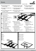
Страница 20: ...5 Press down on the connector and tight en the screws to fix the boad in place Figure 2 1 5 2 2 CHAPTER 2 ...

Страница 21: ...he printer are as follows Be sure to check that the printer operates normally before installing the paper handling controller PCB 1 Turn OFF the printer and reinstall the paper handling controller PCB If the problem is still not rectified conduct the troubleshooting procedures for the various optional I O devices specified in their respective service manuals Notes 1 Refer to the service manual of ...

Страница 22: ......

Страница 23: ...CHAPTER 3 PARTS CATALOG I PAPER HANDLING CONTROLLER PCB ASSEMBLY 3 1 ...

Страница 24: ......

Страница 25: ...ESCRIPTION SERIAL NUMBER REMARKS I 1 2 3 4 5 6 NPN XA9 0836 000 WT2 5391 000 RB1 7071 000 RG1 3707 000 RG5 4314 000 RF1 4083 000 RF 1 2 1 1 1 1 PAPER HANDLING CONTROLLER PCB UNIT SCREW TP M3X6 SCREW HEX PLATE COVER CABLE FLAT PAPER HANDLING CONTROLLER PCB ASS Y IC TMS27C512 12JL EP ROM 1 5 4 6 2 3 ...

Страница 26: ......

Страница 27: ...APPENDIX I PAPER HANDLING CONTROLLER CIRCUIT DIAGRAM A 1 ...

Страница 28: ......

Страница 29: ... HC04 3 2 1 ON OFF JP101 XJBA 0311 JP101S XJBA 0211 IC111 PST591DMT X101 AT 51 8 7 6 5 4 3 2 1 A1 B1 B5 A10 B10 A7 B2 A2 B8 B9 A9 A8 B7 A6 B6 B4 A4 A5 B3 A3 J101 SW101 SSGM14 VCRX VCCLK VCTX VCSTRB UNDET1 UNDET2 PFED SPCHG PDLV VSYNC PRNT N C N C AD 7 0 A 17 8 RD WR 2 6A 2 6D 2 6D 2 6D ASTB 2 6B RESET 60 59 58 57 56 55 54 53 52 51 50 49 48 47 46 45 44 43 42 41 1 2 3 4 5 6 7 8 9 10 11 12 13 14 15 1...

Страница 30: ...1 12 13 14 28 27 26 25 24 23 22 21 20 19 18 17 16 15 A14 A12 A7 A6 A5 A4 A3 A2 A1 A0 I O0 I O1 I O2 Vss Vcc WE A13 A8 A9 A11 OE A10 CS I O7 I O6 I O5 I O4 I O3 6 4 5 0 1 3 2 7 6 5 4 3 0 1 2 5V C120 9 10 8 IC107 HC32 12 13 11 IC107 HC32 IC106 HC04 5 6 8 9 10 WR RD A 17 8 1 2A 1 2B 1 2B 8 IC108 3 4 7 8 13 14 17 18 11 2 5 6 9 12 15 16 19 8D 7D 6D 5D 4D 3D 2D 1D CK 8Q 7Q 6Q 5Q 4Q 3Q 2Q 1Q CLR 1 HC273 ...

Страница 31: ...pared by PERIPHERAL PRODUCTS QUALITY PLANNING DIV PERIPHERAL PRODUCTS TECHNICAL DOCUMENTATION DEPT CANON INC Printed in Japan REVISION 0 JAN 1999 5 1 Hakusan 7 chome Toride City Ibaraki Pref 302 8501 Japan ...

Страница 32: ...PRINTED IN JAPAN IMPRIME AU JAPON 0199AB0 80 CANON INC The printing paper contains 70 waste paper ...

Отзывы: