


Lepton
9
- Technical Information Manual
19
4
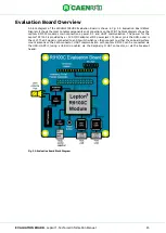
LAYOUT AND COMPONENTS
Introduction
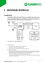
This section describes hardware aspects of embedded RAIN RFID readers based on the Lepton
9
R9100C.
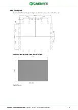
PCB Layout for RF
50 Ohm Characteristic Impedance
As discussed in paragraph
page 12, a properly matched RF connection is critical to achieving
high performance with Lepton
9
R9100C. An improperly matched RF connection will reduce performance in
multiple ways, by both reducing the transmitted RF power, and also increasing the reflected power that
interferes with Lepton
9
R9100C
’s receive circuitry.
When impedance is improperly matched across a node, a signal’s refle
ction coefficient will be proportional
to the difference between the characteristic impedances on both sides of the node divided by their sum, as
shown in the following equation.
Reflection Coefficient of a Load:
In this equation, ZL represents the characteristic impedance of the transmission line, and Z0 represents the
characteristic impedance of the Lepton
9
R9100C, 50 Ohms. For example, if a 40 Ohm transmission line is
used, the reflection coefficient will be = 10 / 90 = 11.1%, thus 11.1% of the power will be reflected back
into the Lepton
9
R9100C, and only 88.9% of the power will be transmitted.
Lepton
9
R9100C is designed to connect to a 50-Ohm characteristic impedance load. The connection
between the Lepton
9
R9100C module and its antennas should all be designed for a 50 Ohm characteristic
impedance. Because the RF connection is made via PCB traces, this requires carefully designing the PCB
layout.
PCB trace characteristic impedance depends on quite a few variables, only some of which can easily be
controlled by the PCB designer. The two main categories of variables are the PCB geometry, and material
properties. PCB geometry includes both the transmission line type, be it microstrip, stripline, or others, and
also the specific dimensions of the forward and return paths and the adjacent dielectrics. Transmission line
styles are shown in
Fig. 4.1: PCB Transmission Line Types
page 19. Material properties to note include the
dielectric constant of the dielectrics in the PCB, and the conductivity of the conductor used.
Fig. 4.1: PCB Transmission Line Types
In most PCB designs, many of the parameters of the PCB are already set, such as dielectric thickness and
constant, trace conductivity and weight, etc. Usually, the only variables that can be easily modified are the