


Lepton
9
- Technical Information Manual
12
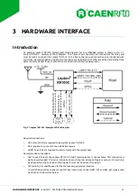
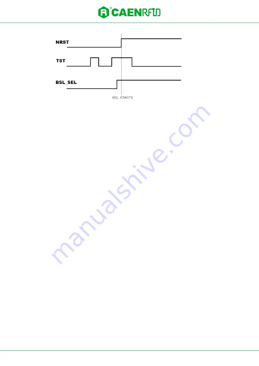
Fig. 3.2: BSL sequence
The BSL program execution starts when TST pin has received a minimum of two positive transitions
and if TST is high while /RST rises from low to high. BSL_SEL shall be at high level before BSL starts.
Pulses length and distance between edges of all signals shall be 10ms at least.
•
UART2 Tx and Rx may be used to examine debug information.
Optional connections:
•
GPIOs allow interaction with the Lepton
9
R9100C as both digital inputs and outputs. They may be used
to trigger inventory, generate events based on inventory activity, or provide general-purpose user-
controlled digital I/O.
•
WKUP provides a mechanism to wake up the Lepton
9
R9100C from the low power Sleep mode. If
unused, this pin should be tied to logic low.
•
UC_ADC allows use of an ADC to convert an analog input voltage into a digital value.
•
UC_DAC allows use of a DAC to generate an analog output voltage from a digital value.
•
RFU is a GPIO reserved for future use.
Power Supply
The Lepton
9
R9100C is powered by a voltage applied to the VDC_IN pin (pin 11) relative to the GND pins.
The supply voltage operating range is 4.75 V to 5.25 V. Current consumption varies from about 1400 mA to
about 5mA depending on the operating mode. The power supply is internally bypassed and regulated, and
no external bypass or bulk storage capacitance is required, as long as the input voltage is stable.
If Lepton
9
R9100C activity is not required at all times, and power reduction is desired, the VDC_IN supply
voltage may be externally gated to remove power to the device.
RF Connection
The Lepton
9
R9100C has a single RF pin (pin 1) which should be connected to a 50
Ω antenna via 50 Ω
controlled impedance connection. This connection could simply be a microstrip transmission line to a PCB
antenna or SMT antenna, or it could include a connector and coaxial cable. The RF connection is single
ended, referenced to ground.
For more information about impedance matching, see
page 19.
UART Communication
The Lepton
9
R9100C has two full-duplex UART standard interfaces, accessible using pins UART1-RX,
UART1-TX, UART2-RX, and UART2-TX. UART1 implements the host communication interface via
easy2read
©
, and UART2 implements the debug interface (RFU). The Tx pins are outputs from the Lepton
9
R9100C, and the Rx pins are inputs to the Lepton
9
R9100C. Both UART interfaces are 921,600 baud, with 8
data bits, 1 stop bit, and no parity bit (8-n-1 configuration).
Each of the UART interfaces signals at 3.3 V relative to GND. The specific VIH, VIL, VOH and VOL
specifications may be found in the §
Device Input and Output Specifications
paragraph page 17. The TX pins
are driven strong high and low with a sink/source current of about 8 mA. If the load on a pin draws more