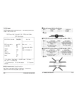
31
GND
32
V-Sync
33
GND
34
Power Good
35
GND
36
PVDD
37
GND
38
PVDD
39
GND
40
PVDD
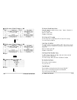
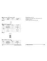
18Bit LCD Panel Pinout
BLUE
GREEN
RED
B0
Æ
NC
G0
Æ
NC
R0
Æ
NC
B1
Æ
NC
G1
Æ
NC
R1
Æ
NC
B2
Æ
B0
G2
Æ
G0
R2
Æ
R0
B3
Æ
B1
G3
Æ
G1
R3
Æ
R1
B4
Æ
B2
G4
Æ
G2
R4
Æ
R2
B5
Æ
B3
G5
Æ
G3
R5
Æ
R3
B6
Æ
B4
G6
Æ
G4
R6
Æ
R4
B7
Æ
B5
G7
Æ
G5
R7
Æ
R5
y
Figure:
1
JTTL1
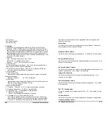
LVDS Panel Signal Pinout: LVDS
Pin#
Assignment
Pin#
Assignment
1
PVDD
2
A4-
3
PVDD
4
A4+
5
A0-
6
A5-
7
A0+
8
A5+
9
A1-
10
A6-
11
A1+
12
A6+
13
A2-
14
A7-
15
A2+
16
A7+
17
A3-
18
CLK2-
19
A3+
20
CLK2+
21
CLK1-
22
GND
23
CLK1+
24
GND
15” Panel PC User’s Manual
P41
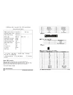
OS Select For DRAM > 64MB:
Select the operating system that is running with greater than 64MB of RAM
on the system.
The choice: Non-OS2, OS2.
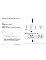
Video BIOS Shadow:
Set Video BIOS Shadow to memory.
The choice: Enabled, Disabled.
Small Logo (EPA) Show:
Set the Logo (EPA) show or not.
The choice: Enabled, Disabled.
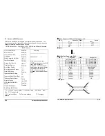
7-6 Advanced Chipset Features
This section allows you to configure the system based on the specific
features of the installed chipset. This chipset manages bus speeds and
access to system memory resources, such as DRAM and the external cache.
It also coordinates communications between the conventional ISA bus and
the PCI bus. It must be stated that these items should never need to be
altered. The default settings have been chosen because they provide the
best operating conditions for your system. The only time you might consider
making any changes would be if you discovered that data was being lost
while using your system.
P16
15” Panel PC User’s Manual


