


SiI
164
PanelLink
Transmitter
Data Sheet
I
2
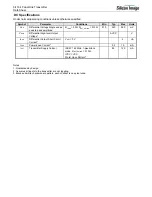
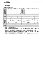
C Register Definitions (cont’d)
Register Name
Access Description
CFG[7:0]
RO
Contains state of inputs D[23:16]. These pins can be used to provide user selectable
configuration data through the I
2
C bus. Only available in 12-bit mode
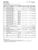
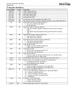
PFEN
RW
PLL Filter Enable in the VDJK Register.
1 – To enable PLL Filter (recommended setting)
0 – To disable PLL Filter
PLLF[3:1]
RW
Set characteristics of PLL filter in the VDJK register
100 – Recommended value
SCNT
RW
SYNC Continuous
1 – To enable (recommended setting)
0 – To disable
DK[3:1]
RW
De-skewing Setting. Increment 260psec.
000 – 1 step -> minimum setup / maximum hold
001 – 2 step
010 – 3 step
011 – 4 step
100 – 5 step -> default (recommended setting)
101 – 6 step
110 – 7 step
111 – 8 step -> maximum setup / minimum hold
Please see Data De-Skew Feature for an illustration
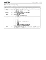
DKEN
RW
De-skewing Enable through DK[3:1] bits. When DKEN pin is HIGH via pin or set to 1,
then De-skew is enabled. When set to 0 De-skew is disabled. Please see Data De-
skew Feature for an illustration.
Содержание DV985S
Страница 1: ...SERVICE MANUAL DV985S...
Страница 6: ...5 1 Optical pickup Unit Explosed View and Part List Pic 1...
Страница 12: ......
Страница 47: ......
Страница 49: ......
Страница 51: ......
Страница 53: ......
Страница 55: ......
Страница 61: ......