background image

VERSION 1.4 

JN30 (38346-X)

Appendix B 

How to flash nano production module with Auvidea JN30B using the NVIDIA SDK manager: 

1. if you use our image form our website, copy the contents of the "JN30" folder to 

/home/USER/nvidia/nvidia_sdk/Jetpack_4.2.2_Linux_GA_P3448-0020/Linux_for_Tegra/


2. connect the JN30B + Nano via micro-USB OTG cable(J12 on the JN30) to the host UBUNTU PC (16.04 or 
higher) 

3. turn on the power for the JN30B -> The nano will now boot in force recovery mode 

4. start the SDK manger 

5. select the Jetson Nano (not the "Jetson Nano (Developer Kit version)“) as target hardware P3448-0020 

(see screenshot) 

6. select the needed Jetpack components 

7. wait until the flashing process is finished


-> first the OS will be flashed to the Nano 


-> after the OS is flashed but before any jetpack components are install the system will boot 


-> follow the end user configuration of the system to set: system language, keyboard layout, 

timezone and user/passwort settings 
 

-> now you can proceed with the installation of the jetpack components


8. Disconnect the micro-USB OTG cable to prevent the system from booting in force recovery mode the next 
time power is turned off and on again.


AUVIDEA GMBH 

TECHNICAL REFERENCE MANUAL 

 18

Содержание 38346

Страница 1: ...38346 X JN30 technical reference manual Version 1 4 Preliminary February 2020 Auvidea GmbH Kellerberg 3 D 86920 Denklingen Tel 49 8243 7714 622 info auvidea com www auvidea com AUVIDEA GMBH TECHNICAL REFERENCE MANUAL 1 ...

Страница 2: ... or any of its contents may be reproduced copied modified or adapted without the prior written consent of the author unless otherwise indicated for stand alone materials You may share this document by any of the following means this PDF file may be distributed freely as long as no changes or modifications to the document are made For any other mode of sharing please contact the author at the email...

Страница 3: ...280 NVME PCIe x4 size 81 7mm x 104 6mm size of the PCB with all components height 21 mm with NVIDIA Nano compute module mounting 4 holes with 3 2mm each model 38346 Power power 12 48V depending on the version more on page 05 The diagram below shows how the ordering code is assembled Models The JN30A is designed for the dev kit version of the Nano compute module The JN30B is designed for the produc...

Страница 4: ...P cameras 38372 M 2 LTE and M 2 Wifi adapter 38385 USB 2 0 to 4x USB 2 0 hub 38391 dev kit camera module and 2x GbE i210 JST GH 38392 dev kit camera module 1x GbE i210 JST GH and mini UPS controller supercaps AUVIDEA GMBH TECHNICAL REFERENCE MANUAL 4 Feature JN30 LC JN30 PD JN30 PSE JN30 PSE48 HDMI out Display port out 48V power in capable micro USB 2 0 OTG USB 3 0 type A 10 100 1000 Ethernet RJ45...

Страница 5: ... that there is no galvanic isolation for the PD power input Potentially this could cause issues if the JN30 is mounted in a metal case with connection to earth ground PSE A JN30 with PoE PSE power sourcing equipment PSE can power a connected PoE device such h as a network IP camera PSE is working with up to 12 95W class 3 Please pay special attention to the temperature of the onboard 12V 48V power...

Страница 6: ...find these beads on the picture below If the beads L34 and or L19 are populated 3 3V is used for CSI If L32 and or L17 populated 5V is used for CSI You can find that option near the CSI connector These components are specially marked with a 3 and a 5 3 3 3V for using Raspberry Pi camera B101 B102 5 5V for using V powered CSI 2 devices AUVIDEA GMBH TECHNICAL REFERENCE MANUAL 6 ...

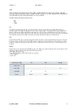
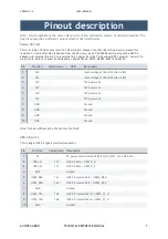
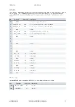
Страница 7: ...8392 Note for best efficiency the 12V rail is set to 10 6V USB 3 0 J11 This is single USB 3 0 type a vertical connector Pin Function Jetson Nano GPIO Description 1 Vdc input voltage of the JN30 max 48V 2 Vdc input voltage of the JN30 max 48V 3 12V 12V power out 4 12V 12V power out 5 12V 12V power out 6 12V 12V power out 7 GND Ground 8 GND Ground 9 GND Ground 10 GND Ground Pin Function Jetson Nano ...

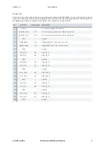
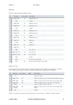
Страница 8: ...lled by USB0_EN_OC A17 max 500 mA 2 USB0 D 109 USB 2 0 data USB2_D_N 3 USB0 D 111 USB 2 0 data USB2_D_P 5 GND Ground Pin Function Jetson Nano Description 1 3 3V 5V 3 3V power supply 5V optional 2 CAM_I2C_SDA 215 3 3V level converted from 1 8V of the Nano 3 CAM_I2C_SCL 213 3 3V level converted from 1 8V of the Nano 4 GND Ground 5 CAM1_MCLK 122 CAM1_MCLK LC 1 8V non LC 3 3V 6 CAM1_PWDN 120 CAM1_PWDN...

Страница 9: ...l 2 CAM_I2C_SDA 215 3 3V level converted from 1 8V of the Nano 3 CAM_I2C_CLK 213 3 3V level converted from 1 8V of the Nano 4 GND Ground 5 CAM0_MCLK 116 CAM0_MCLK LC 1 8V non LC 3 3V 6 CAM0_PWDN 114 CAM0_PWDN LC 1 8V non LC 3 3V 7 GND Ground 8 CSI D_D1 66 CSI4_D3_P 9 CSI D_D1 64 CSI4_D3_N 10 GND Ground 11 CSI D_D0 42 CSI4_D2_P 12 CSI D_D0 40 CSI4_D2_N 13 GND Ground 14 CSI C_CLK 54 CSI4_CLK_P 15 CS...

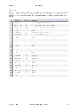
Страница 10: ...no Description 1 3 3V 5V 3 3V power supply default 5V optional 2 GEN2_I2C_SDA 187 3 3V level converted from 1 8V of the Nano 3 GEN2_I2C_SCL 185 3 3V level converted from 1 8V of the Nano 4 GND Ground 5 CAM2_MCLK 116 CAM2_MCLK LC 1 8V non LC 3 3V 6 CAM3_PWDN 118 3 3V level GPIO_01 inverted 7 GND Ground 8 9 10 GND Ground 11 12 13 GND Ground 14 CSI E_CLK 30 CSI2_CLK_P 15 CSI E_CLK 28 CSI2_CLK_N 16 GN...

Страница 11: ...Nano Description 1 3 3V 5V 3 3V power supply 5V optional 2 GEN3_I2C_SDA 232 3 3V level converted from 1 8V of the Nano 3 GEN3_I2C_SCL 234 3 3V level converted from 1 8V of the Nano 4 GND Ground 5 CAM1_MCLK 122 CAM1_MCLK LC 1 8V non LC 3 3V 6 CAM4_PWDN 118 3 3V level GPIO_01 inverted 7 GND Ground 8 9 10 GND Ground 11 12 13 GND Ground 14 CSI F_CLK 29 CSI3_CAM_P 15 CSI F_CLK 27 CSI3_CAM_N 16 GND Grou...

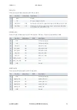
Страница 12: ...MI_TXD0 65 HDMI data lane 0 8 GND Ground 9 HDMI_TXD0 65 HDMI data lane 0 10 HDMI_TXC 83 HDMI clock 11 GND Ground 12 HDMI_TXC 81 HDMI clock 13 HDMI_CEC 94 14 RSVD reserved pin 15 HDMI_DDC_SCL 100 DP1_AUX_CH 16 HDMI_DDC_SDA 98 DP1_AUX_CH 17 GND Ground 18 PWR 5V power max 500 mA 19 HPD 96 inverted and connected to DP1_HPD Pin Function Jetson Nano GPIO Description 1 5V 5V power output 2 UART1_TXD 103 ...

Страница 13: ... PWM control to the fan open drain output controlled by FAN_PWM and disable fan with GPIO19 F2 Pin Function Jetson Nano GPIO Description 1 3 3V 3 3V power supply 2 1 8V 1 8V power supply 3 SPI2_SCK 106 SPI2_SCK 1 8V 4 SPI2_MISO 108 SPI2_MISO 1 8V 5 SPI2_MOSI 104 SPI2_MOSI 1 8V 6 SPI2_CS0 110 SPI2_CS0 1 8V 7 SPI2_CS1 112 SPI2_CS1 1 8V 8 GEN1_I2C_SCL 185 3 3V 9 GEN_1_I2C_SDA 187 3 3V 10 GND Ground P...

Страница 14: ...80 22 x 80 mm Interface four PCIe lanes for top performance no SATA support Recommended Samsung EVO 960 ands 970 modules Pin Function Jetson Nano GPIO Description 1 1 8V 1 8V power supply 2 I2S0_SDIN 195 I2S0_DIN 3 I2S0_SDOUT 193 I2S0_DOUT 4 I2S0_LRCLK 197 I2DS0_FS 5 I2S0_CLK 199 I2S0_SCLK 6 GND Ground Pin Function Jetson Nano GPIO Description 1 1 8V 1 8V power supply 2 I2S1_SDIN 222 I2S1_DIN 3 I2...

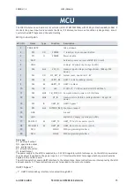
Страница 15: ...RT1 Bypass 1 UART0 Jetson debug interface is tunneled through MCU MCU Pin Name Type Function Description 1 PB8 BOOT0 10k pull down 2 PF0 OD POWER 1 inactive 0 press power button 3 PF1 O POWER Power enable 4 NRST hardware power on reset of MCU RC circuit 5 VddA analog 3 3V supply by always on LDO 6 PA0 Ain0 V12_IN measure input voltage voltage divider 100k up 10k down 7 PA1 OD SYS_RST_IN System res...

Страница 16: ...ST LINK programming adapter SWCLK SWDIO GND We recommend the use of the STM32VLDISCOVERY discovery kit for STM32F100 Value line It is available in the Auvidea online shop and at digikey com 497 10633 ND MCU firmware v1 1 This version of the MCU is limited to a UART baud rate of 38400 baud max Please set the TX1 TX2 to 38400 Please edit the file boot extlinux extlinux conf Please replace 115200n8 b...

Страница 17: ...ually and will not change automatically sudo i2cset y 1 0x20 0x12 0x01 I2cset writes to the I2C device The y part prevents the write confirmation the 1 specifies the I2C bus the 0x20 is the device I2C address of the chip the 0x12 is the register address for the mode configuration and the 0x01 is the value which in this case sets port 1 to manual mode Next to toggle the port on and off there are two...

Страница 18: ...the Jetson Nano not the Jetson Nano Developer Kit version as target hardware P3448 0020 see screenshot 6 select the needed Jetpack components 7 wait until the flashing process is finished first the OS will be flashed to the Nano after the OS is flashed but before any jetpack components are install the system will boot follow the end user configuration of the system to set system language keyboard ...

Страница 19: ...42 card added 3rd mount hole added 3 3V level translation for CSI 2 clk and GPIO signals added I2S connector 1 8V added UART0 connector 1 8V with RTS and CTS added USB host mode for micro USB connector JN30B Revision 5 38346 5 pinout for Nano B01 production module fixed SPI2 pinout see J22 control USB2 and USB3 power by Nano GPIO optional USB 3 power via FanTach GPIO optional added mount hole for ...

Страница 20: ...VERSION 1 4 JN30 38346 X FAQ to be added AUVIDEA GMBH TECHNICAL REFERENCE MANUAL 20 ...

Страница 21: ...al If you have found any typos or errors in this document please let us know This is the preliminary version of this data sheet Please treat all specifications with caution as there may be any typos or errors The Auvidea Team AUVIDEA GMBH TECHNICAL REFERENCE MANUAL 21 ...

Отзывы: