background image

AT90S4414/8515

13

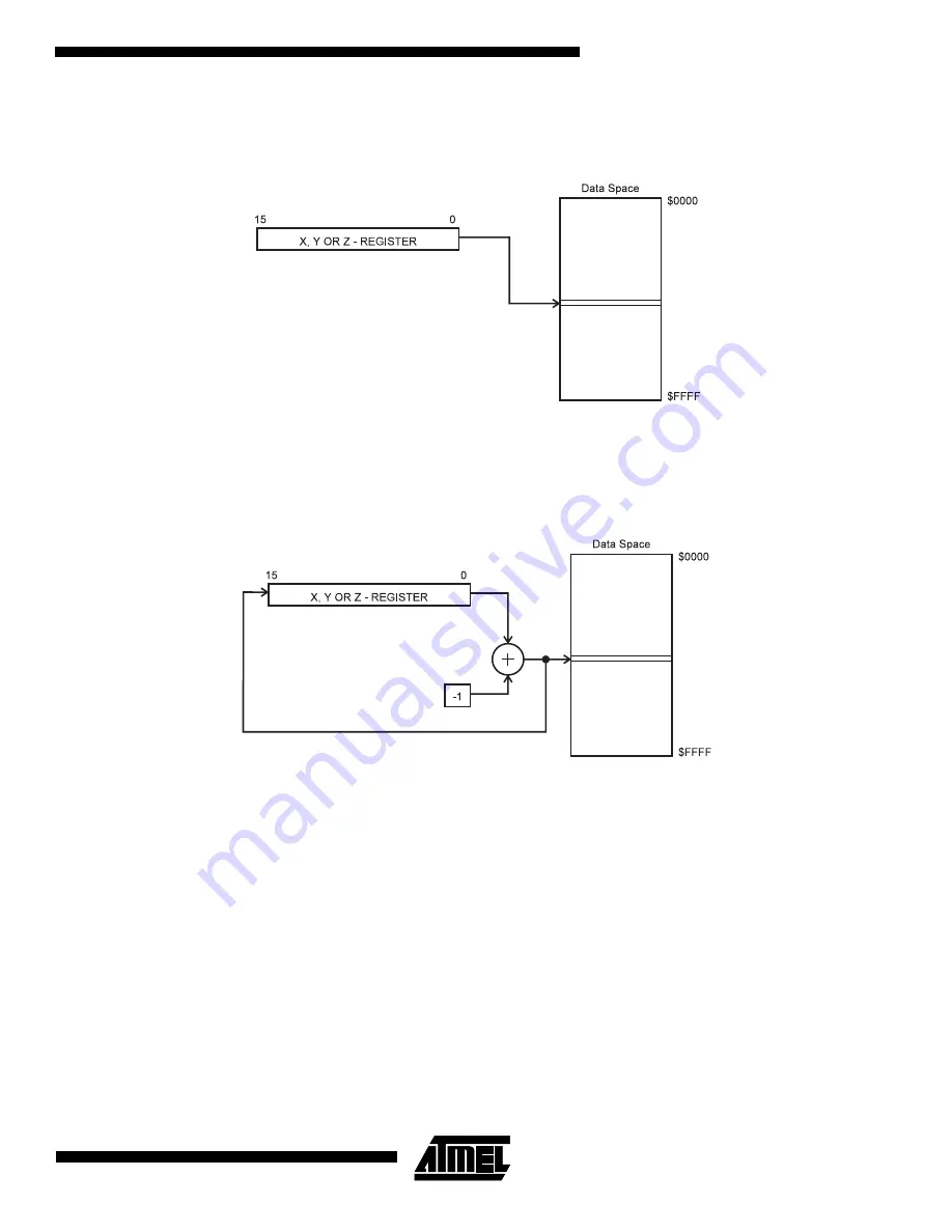
Data Indirect

Figure 14.  Data Indirect Addressing

Operand address is the contents of the X, Y or the Z-register.

Data Indirect with Pre-decrement

Figure 15.  Data Indirect Addressing with Pre-decrement

The X, Y or the Z-register is decremented before the operation. Operand address is the decremented contents of the X, Y
or the Z-register.

Содержание AVR AT90S8515

Страница 1: ...are Capture Modes and Dual 8 9 or 10 bit PWM On chip Analog Comparator Programmable Watchdog Timer with On chip Oscillator Programmable Serial UART Master Slave SPI Serial Interface Special Microcontroller Features Low power Idle and Power Down Modes External and Internal Interrupt Sources Specifications Low power High speed CMOS Process Technology Fully Static Operation Power Consumption at 4 MHz...

Страница 2: ...sed on the AVR RISC architecture By execut ing powerful instructions in a single clock cycle the AT90S4414 8515 achieves throughputs approaching 1 MIPS per MHz allowing the system designer to optimize power consumption versus processing speed Block Diagram Figure 1 The AT90S4414 8515 Block Diagram ...

Страница 3: ...erface or by a conventional nonvolatile memory programmer By combining an enhanced RISC 8 bit CPU with In System Programmable Flash on a monolithic chip the Atmel AT90S4414 8515 is a powerful microcontroller that provides a highly flexible and cost effective solution to many embedded control applications The AT90S4414 8515 AVR is supported with a full suite of program and system development tools ...

Страница 4: ... activated The Port D pins are tri stated when a reset condition becomes active even if the clock is not active Port D also serves the functions of various special features of the AT90S4414 8515 as listed on page 64 RESET Reset input A low level on this pin for more than 50 ns will generate a reset even if the clock is not running Shorter pulses are not guaranteed to generate a reset XTAL1 Input t...

Страница 5: ...nters is also used as the address pointer for the constant table look up function These added function registers are the 16 bits X register Y register and Z register The ALU supports arithmetic and logic functions between registers or between a constant and a register Single register operations are also executed in the ALU Figure 4 shows the AT90S4414 8515 AVR RISC microcontroller architecture In ...

Страница 6: ...in the general data SRAM and consequently the stack size is only limited by the total SRAM size and the usage of the SRAM All user programs must initialize the SP in the reset routine before subroutines or interrupts are executed The 16 bit stack pointer SP is read write accessible in the I O space The 256 512 bytes data SRAM can be easily accessed through the five different addressing modes suppo...

Страница 7: ...ector table at the beginning of the pro gram memory The different interrupts have priority in accordance with their interrupt vector position The lower the interrupt vector address the higher the priority Figure 5 Memory Maps 0000 Data Memory Program Memory 32 Gen Purpose Working Registers 001F 0020 005F 015F 025F 0060 0160 0260 FFFF 64 I O Registers Internal SRAM 256 512 x 8 External SRAM 0 64K X...

Страница 8: ...a Space Although not being physically implemented as SRAM locations this memory organization provides great flexibility in access of the registers as the X Y and Z registers can be set to index any register in the file X Register Y Register And Z Register The registers R26 R31 have some added functions to their general purpose usage These registers are address pointers for indirect addressing of t...

Страница 9: ...words the Flash is organized as 2K x 16 4K x 16 The Flash memory has an endurance of at least 1000 write erase cycles The AT90S4414 8515 Program Counter PC is 11 12 bits wide thus addressing the 2048 4096 program memory addresses See page 77 for a detailed description on Flash data downloading See page 10 for the different program memory addressing modes SRAM Data Memory Internal and External The ...

Страница 10: ...cles whereas interrupt subroutine calls and returns will need four clock cycles more than specified in the instruction set manual The five different addressing modes for the data memory cover Direct Indirect with Displacement Indirect Indirect with Pre Decrement and Indirect with Post Increment In the register file registers R26 to R31 feature the indirect addressing pointer registers The direct a...

Страница 11: ... Register Addressing two registers Operands are contained in register r Rr and d Rd The result is stored in register d Rd I O Direct Figure 11 I O Direct Addressing Operand address is contained in 6 bits of the instruction word n is the destination or source register address ...

Страница 12: ...ined in the 16 LSBs of a two word instruction Rd Rr specify the destination or source register Data Indirect with Displacement Figure 13 Data Indirect with Displacement Operand address is the result of the Y or Z register contents added to the address contained in 6 bits of the instruction word ...

Страница 13: ... address is the contents of the X Y or the Z register Data Indirect with Pre decrement Figure 15 Data Indirect Addressing with Pre decrement The X Y or the Z register is decremented before the operation Operand address is the decremented contents of the X Y or the Z register ...

Страница 14: ... address is the content of the X Y or the Z register prior to incrementing Constant Addressing Using the LPM Instruction Figure 17 Code Memory Constant Addressing Constant byte address is specified by the Z register contents The 15 MSBs select word address 0 2K 4K the LSB selects low byte if cleared LSB 0 or high byte if set LSB 1 000 7FF FFF PROGRAM MEMORY 15 1 0 Z REGISTER ...

Страница 15: ...e 39 specifying the EEPROM address registers the EEPROM data register and the EEPROM control register For the SPI data downloading see page 77 for a detailed description Memory Access Times and Instruction Execution Timing This section describes the general access timing concepts for instruction execution and internal memory access The AVR CPU is driven by the System Clock Ø directly generated fro...

Страница 16: ...d in two System Clock cycles as described in Figure 22 Figure 22 On chip Data SRAM Access Cycles See Interface to External SRAM on page 53 for a description of the access to the external SRAM System Clock Ø 1st Instruction Fetch 1st Instruction Execute 2nd Instruction Fetch 2nd Instruction Execute 3rd Instruction Fetch 3rd Instruction Execute 4th Instruction Fetch T1 T2 T3 T4 System Clock Ø Total ...

Страница 17: ...Timer Counter1 Low Byte 2B 4B OCR1AH Timer Counter1 Output Compare Register A High Byte 2A 4A OCR1AL Timer Counter1 Output Compare Register A Low Byte 29 49 OCR1BH Timer Counter1 Output Compare Register B High Byte 28 48 OCR1BL Timer Counter1 Output Compare Register B Low Byte 25 45 ICR1H T C 1 Input Capture Register High Byte 24 44 ICR1L T C 1 Input Capture Register Low Byte 21 41 WDTCR Watchdog ...

Страница 18: ... the following chapters Status Register SREG The AVR status register SREG at I O space location 3F 5F is defined as Bit 7 I Global Interrupt Enable The global interrupt enable bit must be set one for the interrupts to be enabled The individual interrupt enable control is then performed in separate control registers If the global interrupt enable bit is cleared zero none of the interrupts are enabl...

Страница 19: ...o the data SRAM stack area where the Subroutine and Interrupt Stacks are located This Stack space in the data SRAM must be defined by the program before any subroutine calls are executed or interrupts are enabled The stack pointer must be set to point above 60 The Stack Pointer is decremented by one when data is pushed onto the Stack with the PUSH instruction and it is decremented by two when an a...

Страница 20: ...Handler 00c rjmp ANA_COMP Analog Comparator Handler 00d MAIN ldi r16 high RAMEND Main program start 00e out SPH r16 00f ldi r16 low RAMEND 010 out SPL r16 011 instr xxx Table 3 Reset and Interrupt Vectors Vector No Program Address Source Interrupt Definition 1 000 RESET External Reset Power on Reset and Watchdog Reset 2 001 INT0 External Interrupt Request 0 3 002 INT1 External Interrupt Request 1 ...

Страница 21: ...3 shows the reset logic Table 4 defines the timing and electrical parameters of the reset circuitry Figure 23 Reset Logic Notes 1 The Power on Reset will not work unless the supply voltage has been below VPOT falling The user can select the start up time according to typical oscillator start up The number of WDT oscillator cycles used for each time out is shown in Table 5 The frequency of the watc...

Страница 22: ...be programmed to give a shorter start up time if a ceramic resonator or any other fast start oscillator is used to clock the MCU If the build in start up delay is sufficient RESET can be connected to VCC directly or via an external pull up resistor By holding the pin low for a period after VCC has been applied the Power on Reset period can be extended Refer to Figure 25 for a timing example on thi...

Страница 23: ... the Reset Threshold Voltage VRST on its positive edge the delay timer starts the MCU after the Time out period tTOUT has expired Figure 26 External Reset During Operation Watchdog Reset When the Watchdog times out it will generate a short reset pulse of 1 XTAL cycle duration On the falling edge of this pulse the delay timer starts counting the Time out period tTOUT Refer to page 38 for details on...

Страница 24: ...ternal Interrupt Request 1 Enable When the INT1 bit is set one and the I bit in the Status Register SREG is set one the external pin interrupt is enabled The Interrupt Sense Control1 bits 1 0 ISC11 and ISC10 in the MCU general Control Register MCUCR defines whether the external interrupt is activated on rising or falling edge of the INT1 pin or level sensed Activity on the pin will cause an interr...

Страница 25: ...t Flag Register TIFR Bit 4 Res Reserved bit This bit is a reserved bit in the AT90S4414 8515 and always reads zero Bit 3 TICIE1 Timer Counter1 Input Capture Interrupt Enable When the TICIE1 bit is set one and the I bit in the Status Register is set one the Timer Counter1 Input Capture Event Interrupt is enabled The corresponding interrupt at vector 003 is executed if a capture triggering event occ...

Страница 26: ...ys reads zero External Interrupts The external interrupts are triggered by the INT1 and INT0 pins Observe that if enabled the interrupts will trigger even if the INT0 INT1 pins are configured as outputs This feature provides a way of generating a software interrupt The external interrupts can be triggered by a falling or rising edge or a low level This is set up as indicated in the specification f...

Страница 27: ...st before the execution of the SLEEP instruction Bit 4 SM Sleep Mode This bit selects between the two available sleep modes When SM is cleared zero Idle Mode is selected as Sleep Mode When SM is set one Power Down mode is selected as sleep mode For details refer to the paragraph Sleep Modes below Bit 3 2 ISC11 ISC10 Interrupt Sense Control 1 bit 1 and bit 0 The External Interrupt 1 is activated by...

Страница 28: ...iggered interrupts as well as internal ones like Timer Overflow interrupt and watchdog reset If wakeup from the Analog Comparator interrupt is not required the analog comparator can be powered down by setting the ACD bit in the Analog Comparator Control and Status register ACSR This will reduce power consumption in Idle Mode When the MCU wakes up from Idle mode the CPU starts program execution imm...

Страница 29: ... Counter Insterrupt Flag Register TIFR Control signals are found in the Timer Counter0 Control Register TCCR0 The interrupt enable disable settings for Timer Counter0 are found in the Timer Counter Interrupt Mask Register TIMSK When Timer Counter0 is externally clocked the external signal is synchronized with the oscillator frequency of the CPU To assure proper sampling of the external clock the m...

Страница 30: ...0 bit 2 1 and 0 The Clock Select0 bits 2 1 and 0 define the prescaling source of Timer Counter0 Bit 7 6 5 4 3 2 1 0 33 53 CS02 CS01 CS00 TCCR0 Read Write R R R R R R W R W R W Initial value 0 0 0 0 0 0 0 0 Table 8 Clock 0 Prescale Select CS02 CS01 CS00 Description 0 0 0 Stop the Timer Counter0 is stopped 0 0 1 CK 0 1 0 CK 8 0 1 1 CK 64 1 0 0 CK 256 1 0 1 CK 1024 1 1 0 External Pin T0 falling edge ...

Страница 31: ...ve the user SW control of the counting Timer Counter 0 TCNT0 The Timer Counter0 is realized as an up counter with read and write access If the Timer Counter0 is written and a clock source is present the Timer Counter0 continues counting in the clock cycle following the write operation 16 bit Timer Counter1 Figure 30 shows the block diagram for Timer Counter1 Figure 30 Timer Counter1 Block Diagram ...

Страница 32: ...sed as a 8 9 or 10 bit Pulse With Modulator In this mode the counter and the OCR1A OCR1B registers serve as a dual glitch free stand alone PWM with centered pulses Refer to page 41 for a detailed description on this function The Input Capture function of Timer Counter1 provides a capture of the Timer Counter1 contents to the Input Capture Register ICR1 triggered by an external event on the Input C...

Страница 33: ...in the ICES1 bit The actual sampling frequency is XTAL clock frequency Bit 6 ICES1 Input Capture1 Edge Select While the ICES1 bit is cleared zero the Timer Counter1 contents are transferred to the Input Capture Register ICR1 on the falling edge of the input capture pin ICP While the ICES1 bit is set one the Timer Counter1 contents are transferred to the Input Capture Register ICR1 on the rising ed...

Страница 34: ...ing Timer Counter1 TCNT1H AND TCNT1L This 16 bit register contains the prescaled value of the 16 bit Timer Counter1 To ensure that both the high and low bytes are read and written simultaneously when the CPU accesses these registers the access is performed using an 8 bit temporary register TEMP This temporary register is also used when accessing OCR1A OCR1B and ICR1 If the main program and also in...

Страница 35: ... OCR1B to the same value does not generate a compare match A compare match will set the compare interrupt flag in the CPU clock cycle following the compare event Since the Output Compare Registers OCR1A and OCR1B are 16 bit registers a temporary register TEMP is used when OCR1A B are written to ensure that both bytes are updated simultaneously When the CPU writes the high byte OCR1AH or OCR1BH the...

Страница 36: ...wed from within interrupt routines Timer Counter1 In PWM Mode When the PWM mode is selected Timer Counter1 and the Output Compare Register1A OCR1A and the Output Compare Register1B OCR1B form a dual 8 9 or 10 bit free running glitch free and phase correct PWM with outputs on the PD5 OC1A and OC1B pins Timer Counter1 acts as an up down counter counting up from 0000 to TOP see Table 12 where it turn...

Страница 37: ... or TOP the output OC1A OC1B is updated to low or high on the next compare match according to the settings of COM1A1 COM1A0 or COM1B1 COM1B0 This is shown in Table Note X A or B In PWM mode the Timer Overflow Flag1 TOV1 is set when the counter advances from 0000 Timer Overflow Interrupt1 operates exactly as in normal Timer Counter mode i e it is executed when TOV1 is set provided that Timer Overfl...

Страница 38: ...g Timer Watchdog Timer Control Register WDTCR Bits 7 5 Res Reserved bits These bits are reserved bits in the AT90S4414 8515 and will always read as zero Bit 4 WDTOE Watch Dog Turn Off Enable This bit must be set one when the WDE bit is cleared Otherwise the watchdog will not be disabled Once set hardware will clear this bit to zero after four clock cycles Refer to the description of the WDE bit fo...

Страница 39: ...se conditions is likely cause the program counter to perform unintentional jumps and eventually execute the EEPROM write code To secure EEPROM integrity the user is advised to use an external under voltage reset circuit in this case In order to prevent unintentional EEPROM writes a specific write procedure must be followed Refer to the description of the EEPROM Control Register for details on this...

Страница 40: ...to EEWE otherwise no EEPROM write takes place The following procedure should be followed when writing the EEPROM the order of steps 2 and 3 is unessential 1 Wait until EEWE becomes zero 2 Write new EEPROM address to EEARL and EEARH optional 3 Write new EEPROM data to EEDR optional 4 Write a logical one to the EEMWE bit in EECR 5 Within four clock cycles after setting EEMWE write a logical one to E...

Страница 41: ...execute instructions incor rectly if the supply voltage for executing instructions is too low EEPROM data corruption can easily be avoided by following these design recommendations one is sufficient 1 Keep the AVR RESET active low during periods of insufficient power supply voltage This is best done by an exter nal low VCC Reset Protection circuit often referred to as a Brown Out Detector BOD Plea...

Страница 42: ...hifting one byte the SPI clock generator stops setting the end of transmission flag SPIF If the SPI interrupt enable bit SPIE in the SPCR register is set an interrupt is requested The Slave Select input PB4 SS is set low to select an individual slave SPI device The two shift registers in the Master and the Slave can be considered as one distributed 16 bit circular shift register This is shown in F...

Страница 43: ...selecting the SPI as a slave and starting to send data to it To avoid bus contention the SPI system takes the following actions 1 The MSTR bit in SPCR is cleared and the SPI system becomes a slave As a result of the SPI becoming a slave the MOSI and SCK pins become inputs 2 The SPIF flag in SPSR is set and if the SPI interrupt is enabled and the I bit in SREG are set the interrupt routine will be ...

Страница 44: ...E SPI Enable When the SPE bit is set one the SPI is enabled This bit must be set to enable any SPI operations Bit 5 DORD Data Order When the DORD bit is set one the LSB of the data word is transmitted first When the DORD bit is cleared zero the MSB of the data word is transmitted first Bit 4 MSTR Master Slave Select This bit selects Master SPI mode when set one and Slave SPI mode when cleared zero...

Страница 45: ...ter when SPIF is set one then accessing the SPI Data Register SPDR Bit 6 WCOL Write Collision Flag The WCOL bit is set if the SPI data register SPDR is written during a data transfer The WCOL bit and the SPIF bit are cleared zero by first reading the SPI Status Register when WCOL is set one and then accessing the SPI Data Register Bit 5 0 Res Reserved bits These bits are reserved bits in the AT90S...

Страница 46: ... generator that can generate a large number of baud rates bps High baud rates at low XTAL frequencies 8 or 9 bits data Noise filtering Overrun detection Framing Error detection False Start Bit detection Three separate interrupts on TX Complete TX Data Register Empty and RX Complete Data Transmission A block schematic of the UART transmitter is shown in Figure 38 Figure 38 UART Transmitter ...

Страница 47: ...t and bit 9 or 10 is set stop bit If 9 bit data word is selected the CHR9 bit in the UART Control Register UCR is set the TXB8 bit in UCR is transferred to bit 9 in the Transmit shift register On the Baud Rate clock following the transfer operation to the shift register the start bit is shifted out on the TXD pin Then follows the data LSB first When the stop bit has been shifted out the shift regi...

Страница 48: ...ansmit Data register is accessed If 9 bit data word is selected the CHR9 bit in the UART Control Register UCR is set the RXB8 bit in UCR is loaded with bit 9 in the Transmit shift register when data is transferred to UDR If after having received a character the UDR register has not been read since the last receive the OverRun OR flag in UCR is set This means that the last data byte shifted into to...

Страница 49: ...it in UCR is set the UART Transmit Complete interrupt to be executed as long as UDRE is set UDRE is cleared by writing UDR When interrupt driven data transmittal is used the UART Data Register Empty Interrupt routine must write UDR in order to clear UDRE otherwise a new interrupt will occur once the interrupt routine terminates UDRE is set one during reset to indicate that the transmitter is ready...

Страница 50: ...nd received characters are 9 bit long plus start and stop bits The 9th bit is read and written by using the RXB8 and TXB8 bits in UCR respectively The 9th data bit can be used as an extra stop bit or a parity bit Bit 1 RXB8 Receive Data Bit 8 When CHR9 is set one RXB8 is the 9th data bit of the received character Bit 0 TXB8 Transmit Data Bit 8 When CHR9 is set one TXB8 is the 9th data bit in the c...

Страница 51: ... MHz Error 4 MHz Error 4 608 MHz Error 2400 UBRR 84 0 4 UBRR 95 0 0 UBRR 103 0 2 UBRR 119 0 0 4800 UBRR 42 0 8 UBRR 47 0 0 UBRR 51 0 2 UBRR 59 0 0 9600 UBRR 20 1 6 UBRR 23 0 0 UBRR 25 0 2 UBRR 29 0 0 14400 UBRR 13 1 6 UBRR 15 0 0 UBRR 16 2 1 UBRR 19 0 0 19200 UBRR 10 3 1 UBRR 11 0 0 UBRR 12 0 2 UBRR 14 0 0 28800 UBRR 6 1 6 UBRR 7 0 0 UBRR 8 3 7 UBRR 9 0 0 38400 UBRR 4 6 3 UBRR 5 0 0 UBRR 6 7 5 UBR...

Страница 52: ...r Interrupt must be disabled by clearing the ACIE bit in ACSR Otherwise an interrupt can occur when the bit is changed Bit 6 Res Reserved bit This bit is a reserved bit in the AT90S4414 8515 and will always read as zero Bit 5 ACO Analog Comparator Output ACO is directly connected to the comparator output Bit 4 ACI Analog Comparator Interrupt Flag This bit is set one when a comparator output event ...

Страница 53: ...CR MCU control register and will override the setting of the data direction register DDRA When the SRE bit is cleared zero the external data SRAM is disabled and the normal pin and data direction settings are used When SRE is cleared zero the address space above the internal SRAM boundary is not mapped into the internal SRAM as in AVR parts not having interface to the external SRAM When ALE goes f...

Страница 54: ... RD WR SRAM D Q G Port A ALE Port C RD WR AVR System Clock Ø ALE WR RD Data Address 7 0 Data Address 7 0 Address 15 8 Address Address Address T1 T2 T3 Prev Address Prev Address Prev Address Data Data Write Read Address Address System Clock Ø ALE WR RD Data Address 7 0 Data Address 7 0 Address 15 8 Address Address Address T1 T2 T3 T4 Prev Address Prev Address Prev Address Data Data Write Read Addr ...

Страница 55: ...E External SRAM Enable bit in the MCUCR MCU Control Register the alternate settings override the data direction register Port A Data Register PORTA Port A Data Direction Register DDRA Port A Input Pins Address PINA The Port A Input Pins address PINA is not a register and this address enables access to the physical value on each Port A pin When reading PORTA the Port A Data Latch is read and when r...

Страница 56: ...n latch is however not shown in the figure Figure 45 Port A Schematic Diagrams Pins PA0 PA7 Table 20 DDAn Effects on Port A Pins DDAn PORTAn I O Pull up Comment 0 0 Input No Tri state Hi Z 0 1 Input Yes PAn will source current if ext pulled low 1 0 Output No Push Pull Zero Output 1 1 Output No Push Pull One Output ...

Страница 57: ... B Input Pins Address PINB The Port B Input Pins address PINB is not a register and this address enables access to the physical value on each Port B pin When reading PORTB the Port B Data Latch is read and when reading PINB the logical values present on the pins are read Table 21 Port B Pins Alternate Functions Port Pin Alternate Functions PB0 T0 Timer Counter 0 external counter input PB1 T1 Timer...

Страница 58: ...rt B Bit 5 MOSI SPI Master data output slave data input for SPI channel When the SPI is enabled as a slave this pin is configured as an input regardless of the setting of DDB5 When the SPI is enabled as a master the data direction of this pin is con trolled by DDB5 When the pin is forced to be an input the pull up can still be controlled by the PORTB5 bit See the description of the SPI port for fu...

Страница 59: ...he figures Figure 46 Port B Schematic Diagram Pins PB0 and PB1 Figure 47 Port B Schematic Diagram Pins PB2 and PB3 DATA BUS D D Q Q RESET RESET C C WD WP RD MOS PULL UP PBn R R WP WD RL RP RD WRITE PORTB WRITE DDRB READ PORTB LATCH READ PORTB PIN READ DDRB DDBn PORTBn SENSE CONTROL TIMERn CLOCK SOURCE MUX CSn2 CSn0 RL RP CSn1 n 0 1 ...

Страница 60: ...TR SPE WP WD RL RP RD MSTR SPE WRITE PORTB WRITE DDRB READ PORTB LATCH READ PORTB PIN READ DDRB SPI MASTER ENABLE SPI ENABLE DDB4 PORTB4 RL RP DATA BUS D D Q Q RESET RESET C C WD WP RD MOS PULL UP PB5 R R WP WD RL RP RD SPE MSTR WRITE PORTB WRITE DDRB READ PORTB LATCH READ PORTB PIN READ DDRB SPI ENABLE MASTER SELECT DDB5 PORTB5 SPE MSTR SPI MASTER OUT SPI SLAVE IN RL RP ...

Страница 61: ...SPE MSTR WRITE PORTB WRITE DDRB READ PORTB LATCH READ PORTB PIN READ DDRB SPI ENABLE MASTER SELECT DDB6 PORTB6 SPE MSTR SPI SLAVE OUT SPI MASTER IN RL RP DATA BUS D D Q Q RESET RESET C C WD WP RD MOS PULL UP PB7 R R WP WD RL RP RD SPE MSTR WRITE PORTB WRITE DDRB READ PORTB LATCH READ PORTB PIN READ DDRB SPI ENABLE MASTER SELECT DDB7 PORTB7 SPE MSTR SPI CLOCK OUT SPI CLOCK IN RL RP ...

Страница 62: ...g PORTC the Port C Data Latch is read and when reading PINC the logical values present on the pins are read PortC as General Digital I O All 8 pins in Port C have equal functionality when used as digital I O pins PCn General I O pin The DDCn bit in the DDRC register selects the direction of this pin if DDCn is set one PCn is con figured as an output pin If DDCn is cleared zero PCn is configured as...

Страница 63: ...ata Direction Register are read write The Port D output buffers can sink 20 mA As inputs Port D pins that are externally pulled low will source current if the pull up resistors are activated Some Port D pins have alternate functions as shown in the following table When the pins are used for the alternate function the DDRD and PORTD register has to be set according to the alternate function descrip...

Страница 64: ...l SRAM on page 53 for detailed information WR Port D Bit 6 WR is the external data memory write control strobe See Interface to External SRAM on page 53 for detailed information OC1A Port D Bit 5 OC1A Output compare match output The PD5 pin can serve as an external output when the Timer Counter1 compare matches The PD5 pin has to be configured as an output DDD5 set one to serve this function See t...

Страница 65: ...is pin is configured as an output regardless of the value of DDRD1 RXD Port D Bit 0 Receive Data Data input pin for the UART When the UART receiver is enabled this pin is configured as an input regard less of the value of DDRD0 When the UART forces this pin to be an input a logical one in PORTD0 will turn on the internal pull up PortD Schematics Note that all port pins are synchronized The synchro...

Страница 66: ...ure 55 Port D Schematic Diagram Pins PD2 and PD3 DATA BUS D D Q Q RESET RESET C C WD WP RD RP RL MOS PULL UP PD1 R R WP WD RL RP RD TXD TXEN WRITE PORTD WRITE DDRD READ PORTD LATCH READ PORTD PIN READ DDRD UART TRANSMIT DATA UART TRANSMIT ENABLE DDD1 PORTD1 TXEN TXD ...

Страница 67: ...AT90S4414 8515 67 Figure 56 Port D Schematic Diagram Pin PD4 Figure 57 Port D Schematic Diagram Pin PD5 ...

Страница 68: ...AT90S4414 8515 68 Figure 58 Port D Schematic Diagram Pin PD6 Figure 59 Port D Schematic Diagram Pin PD7 ...

Страница 69: ... manufactured by Atmel 2 001 93 indicates 8KB Flash memory 3 002 01 indicates AT90S8515 device when signature byte 001 is 93 For the AT90S4414 1 they are 1 000 1E indicates manufactured by Atmel 2 001 92 indicates 4KB Flash memory 3 002 01 indicates AT90S4414 device when signature byte 001 is 92 Note 1 When both Lock bits are programmed Lock mode 3 the signature bytes can not be read in serial mod...

Страница 70: ...8515 are referenced by signal names describing their function during parallel programming See Figure 60 and Table 28 Pins not described in Table 28 are referenced by pin names The XA1 XA0 pins determine the action executed when the XTAL1 pin is given a positive pulse The bit coding are shown in Table 29 When pulsing WR or OE the command loaded determines the action executed The Command is a byte w...

Страница 71: ...put Enable Active low WR PD3 I Write Pulse Active low BS PD4 I Byte Select 0 selects low byte 1 selects high byte XA0 PD5 I XTAL Action Bit 0 XA1 PD6 I XTAL Action Bit 1 DATA PB7 0 I O Bidirectional Databus Output when OE is low Table 29 XA1 and XA0 Coding XA1 XA0 Action when XTAL1 is Pulsed 0 0 Load Flash or EEPROM Address High or low address byte determined by BS 0 1 Load Data High or Low data b...

Страница 72: ...gh Byte 1 Set XA1 XA0 to 00 This enables address loading 2 Set BS to 1 This selects high byte 3 Set DATA Address high byte 00 07 0F 4 Give XTAL1 a positive pulse This loads the address high byte C Load Address Low Byte 1 Set XA1 XA0 to 00 This enables address loading 2 Set BS to 0 This selects low byte 3 Set DATA Address low byte 00 FF 4 Give XTAL1 a positive pulse This loads the address low byte ...

Страница 73: ...cations Address high byte needs only be loaded before programming a new 256 word page in the Flash Skip writing the data value FF that is the contents of the entire Flash and EEPROM after a Chip Erase These considerations also applies to EEPROM programming and Flash EEPROM and Signature bytes reading Figure 61 Programming the Flash Waveforms Figure 62 Programming the Flash Waveforms continued 10 A...

Страница 74: ...00 FF 5 E Write Data Low Byte Reading the EEPROM The algorithm for reading the EEPROM memory is as follows refer to Programming the Flash for details on Command and Address loading 1 A Load Command 0000 0011 2 AT90S8515 only B Load Address High Byte 00 01 3 C Load Address Low Byte 00 FF 4 Set OE to 0 and BS to 0 The EEPROM data byte can now be read at DATA 5 Set OE to 1 Programming the Fuse Bits T...

Страница 75: ...m for reading the Fuse and Lock bits is as follows refer to Programming the Flash for details on Command loading 1 A Load Command 0000 0100 2 Set OE to 0 and BS to 1 The status of the Fuse and Lock bits can now be read at DATA 0 means programmed Bit 7 Lock Bit1 Bit 6 Lock Bit2 Bit 5 SPIEN Fuse bit Bit 0 FSTRT Fuse bit 3 Set OE to 1 Observe that BS needs to be set to 1 Reading the Signature Bytes T...

Страница 76: ...7 ns tXHXL XTAL1 Pulse Width High 67 ns tXLDX Data and Control Hold after XTAL1 Low 67 ns tXLWL XTAL1 Low to WR Low 67 ns tBVWL BS Valid to WR Low 67 ns tRHBX BS Hold after RDY BSY High 67 ns tWLWH WR Pulse Width Low 1 67 ns tWHRL WR High to RDY BSY Low 2 20 ns tWLRH WR Low to RDY BSY High 2 0 5 0 7 0 9 ms tXLOL XTAL1 Low to OE Low 67 ns tOLDV OE Low to DATA Valid 20 ns tOHDZ OE High to DATA Tri s...

Страница 77: ...eed to first exe cute the Chip Erase instruction The Chip Erase instruction turns the content of every memory location in both the Program and EEPROM arrays into FF The Program and EEPROM memory arrays have separate address spaces 0000 to 07FF 0FFF AT90S4414 8515 for Program memory and 0000 to 00FF 01FF AT90S4414 8515 for EEPROM memory Either an external clock is supplied at pin XTAL1 or a crystal...

Страница 78: ...e Table 35 on page 80 for tWD_ERASE value 5 The Flash or EEPROM array is programmed one byte at a time by supplying the address and data together with the appropriate Write instruction An EEPROM memory location is first automatically erased before new data is written Use Data Polling to detect when the next byte in the Flash or EEPROM can be written If polling is not used wait tWD_PROG before tran...

Страница 79: ... both Lock bits programmed Table 33 Serial Programming Instruction Set Instruction Instruction Format Operation Byte 1 Byte 2 Byte 3 Byte4 Programming Enable 1010 1100 0101 0011 xxxx xxxx xxxx xxxx Enable Serial Programming while RESET is low Chip Erase 1010 1100 100x xxxx xxxx xxxx xxxx xxxx Chip Erase Flash and EEPROM memory arrays Read Program Memory 0010 H000 xxxx aaaa bbbb bbbb oooo oooo Read...

Страница 80: ...C 4 0 6 0V 0 8 MHz tCLCL Oscillator Period VCC 4 0 6 0V 125 ns tSHSL SCK Pulse Width High 2 tCLCL ns tSLSH SCK Pulse Width Low 2 tCLCL ns tOVSH MOSI Setup to SCK High tCLCL ns tSHOX MOSI Hold after SCK High 2 tCLCL ns tSLIV SCK Low to MISO Valid 10 16 32 ns Table 35 Minimum Wait Delay after the Chip Erase Instruction Symbol 3 2V 3 6V 4 0V 5 0V tWD_ERASE 18 ms 14 ms 12 ms 8 ms Table 36 Minimum Wait...

Страница 81: ...evice at these or other conditions beyond those indicated in the operational sections of this specification is not implied Exposure to absolute maximum rating conditions for extended periods may affect device reliability Storage Temperature 65 C to 150 C Voltage on any Pin except RESET with respect to Ground 1 0V to VCC 0 5V Voltage on RESET with respect to Ground 1 0V to 13 0V Maximum Operating V...

Страница 82: ...ceed 100 mA If IOH exceeds the test condition VOH may exceed the related specification Pins are not guaranteed to source current greater than the listed test condition 5 Minimum VCC for Power Down is 2V TA 40 C to 85 C VCC 2 7V to 6 0V unless otherwise noted Symbol Parameter Condition Min Typ Max Units VIL Input Low Voltage Except XTAL1 0 5 0 3 VCC 1 V VIL1 Input Low Voltage XTAL1 0 5 0 2 VCC 1 V ...

Страница 83: ...CC 2 7V to 4 0V VCC 4 0V to 6 0V Units Min Max Min Max 1 tCLCL Oscillator Frequency 0 4 0 8 MHz tCLCL Clock Period 250 125 ns tCHCX High Time 100 50 ns tCLCX Low Time 100 50 ns tCLCH Rise Time 1 6 0 5 µs tCHCL Fall Time 1 6 0 5 µs VIL1 VIH1 System Clock O ALE WR RD Data Address 7 0 Data Address 7 0 Address 15 8 Address Address Address T1 T2 T3 T4 Prev Address Prev Address Prev Address 1 0 4 2 13 3...

Страница 84: ... Low 95 0 1 0tCLCL 30 0 ns 6 tAVWL Address Valid to WR Low 157 5 1 5tCLCL 30 0 1 ns 7 tLLWL ALE Low to WR Low 105 0 145 1 0tCLCL 20 0 1 0tCLCL 20 0 ns 8 tLLRL ALE Low to RD Low 42 5 82 5 0 5tCLCL 20 0 2 0 5tCLCL 20 0 2 ns 9 tDVRH Data Setup to RD High 60 0 60 0 ns 10 tRLDV Read Low to Data Valid 70 0 1 0tCLCL 55 0 ns 11 tRHDX Data Hold After RD High 0 0 0 0 ns 12 tRLRH RD Pulse Width 105 0 1 0tCLC...

Страница 85: ...L 50 0 ns 6 tAVWL Address Valid to WR Low 325 0 1 5tCLCL 50 0 1 ns 7 tLLWL ALE Low to WR Low 230 0 270 0 1 0tCLCL 20 0 1 0tCLCL 20 0 ns 8 tLLRL ALE Low to RD Low 105 0 145 0 0 5tCLCL 20 0 2 0 5tCLCL 20 0 2 ns 9 tDVRH Data Setup to RD High 95 0 95 0 ns 10 tRLDV Read Low to Data Valid 170 0 1 0tCLCL 80 0 ns 11 tRHDX Data Hold After RD High 0 0 0 0 ns 12 tRLRH RD Pulse Width 230 0 1 0tCLCL 20 0 ns 13...

Страница 86: ...actors are operating voltage and frequency The current drawn from capacitive loaded pins may be estimated for one pin as CL VCC f where CL load capacitance VCC operating voltage and f average switching frequency of I O pin The parts are characterized at frequencies higher than test limits Parts are not guaranteed to function properly at frequen cies higher than the ordering code indicates The diff...

Страница 87: ...0 12 14 2 2 5 3 3 5 4 4 5 5 5 5 6 ACTIVE SUPPLY CURRENT vs Vcc FREQUENCY 4 MHz I cc mA Vcc V T 85 C A T 25 C A T 40 C A 0 2 4 6 8 10 12 0 1 2 3 4 5 6 7 8 9 10 11 12 13 14 15 Vcc 6V Vcc 5 5V Vcc 5V Vcc 4 5V Vcc 4V Vcc 3 6V Vcc 3 3V Vcc 3 0V Vcc 2 7V IDLE SUPPLY CURRENT vs FREQUENCY T 25 C A Frequency MHz I cc mA ...

Страница 88: ... vs VCC 0 0 5 1 1 5 2 2 5 3 3 5 4 2 2 5 3 3 5 4 4 5 5 5 5 6 T 25 C A T 85 C A IDLE SUPPLY CURRENT vs Vcc I cc mA Vcc V FREQUENCY 4 MHz T 40 C A 0 2 4 6 8 10 12 2 2 5 3 3 5 4 4 5 5 5 5 6 T 85 C A T 25 C A POWER DOWN SUPPLY CURRENT vs Vcc I cc µΑ Vcc V WATCHDOG TIMER DISABLED T 45 C A T 70 C A ...

Страница 89: ... Current vs VCC 0 20 40 60 80 100 120 140 2 2 5 3 3 5 4 4 5 5 5 5 6 T 85 C A T 25 C A POWER DOWN SUPPLY CURRENT vs Vcc I cc µΑ Vcc V WATCHDOG TIMER ENABLED 0 0 1 0 2 0 3 0 4 0 5 0 6 0 7 0 8 2 2 5 3 3 5 4 4 5 5 5 5 6 ANALOG COMPARATOR CURRENT vs Vcc I cc mA Vcc V T 25 C A T 85 C A T 40 C A ...

Страница 90: ...r Offset Voltage vs Common Mode Voltage 0 2 4 6 8 10 12 14 16 18 0 0 5 1 1 5 2 2 5 3 3 5 4 4 5 5 ANALOG COMPARATOR OFFSET VOLTAGE vs V 5V cc COMMON MODE VOLTAGE Common Mode Voltage V Offset Voltage mV T 85 C A T 25 C A 0 2 4 6 8 10 0 0 5 1 1 5 2 2 5 3 ANALOG COMPARATOR OFFSET VOLTAGE vs COMMON MODE VOLTAGE Common Mode Voltage V Offset Voltage mV V 2 7V cc T 85 C A T 25 C A ...

Страница 91: ...tor Frequency vs VCC 60 50 40 30 20 10 0 10 0 0 5 1 5 1 2 2 5 3 5 3 4 4 5 5 6 6 5 7 5 5 ANALOG COMPARATOR INPUT LEAKAGE CURRENT T 25 C A I nA ACLK V V IN V 6V CC 0 200 400 600 800 1000 1200 1400 1600 2 2 5 3 3 5 4 4 5 5 5 5 6 T 85 C A T 25 C A WATCHDOG OSCILLATOR FREQUENCY vs Vcc V V cc F KHz RC ...

Страница 92: ... vs Input Voltage Figure 81 Pull up Resistor Current vs Input Voltage 0 20 40 60 80 100 120 0 0 5 1 1 5 2 2 5 3 3 5 4 4 5 5 PULL UP RESISTOR CURRENT vs INPUT VOLTAGE V 5V cc I µA OP V V OP T 85 C A T 25 C A 0 5 10 15 20 25 30 0 0 5 1 1 5 2 2 5 3 PULL UP RESISTOR CURRENT vs INPUT VOLTAGE I µA OP V V OP V 2 7V cc T 85 C A T 25 C A ...

Страница 93: ...e Current vs Output Voltage 0 10 20 30 40 50 60 70 0 0 5 1 1 5 2 2 5 3 V 5V cc I mA OL V V OL T 85 C A T 25 C A I O PIN SINK CURRENT vs OUTPUT VOLTAGE 0 2 4 6 8 10 12 14 16 18 20 0 0 5 1 1 5 2 2 5 3 3 5 4 4 5 5 I O PIN SOURCE CURRENT vs OUTPUT VOLTAGE V 5V cc I mA OH V V OH T 85 C A T 25 C A ...

Страница 94: ... Figure 85 I O Pin Input Threshold Voltage vs VCC 0 1 2 3 4 5 6 0 0 5 1 1 5 2 2 5 3 I O PIN SOURCE CURRENT vs OUTPUT VOLTAGE I mA OH V V OH T 85 C A T 25 C A V 2 7V cc 0 0 5 1 1 5 2 2 5 2 7 4 0 5 0 Threshold Voltage V Vcc I O PIN INPUT THRESHOLD VOLTAGE vs Vcc T 25 C A ...

Страница 95: ...I O Pin Sink Current vs Output Voltage 0 0 02 0 04 0 06 0 08 0 1 0 12 0 14 0 16 0 18 2 7 4 0 5 0 Input hysteresis V Vcc I O PIN INPUT HYSTERESIS vs Vcc T 25 C A 0 5 10 15 20 25 0 0 5 1 1 5 2 I mA OL V V OL T 85 C A T 25 C A I O PIN SINK CURRENT vs OUTPUT VOLTAGE V 2 7V cc ...

Страница 96: ... Low Byte 35 29 49 OCR1BH Timer Counter1 Output Compare Register B High Byte 35 28 48 OCR1BL Timer Counter1 Output Compare Register B Low Byte 35 Reserved 25 45 ICR1H Timer Counter1 Input Capture Register High Byte 36 24 44 ICR1L Timer Counter1 Input Capture Register Low Byte 36 Reserved 21 41 WDTCR WDTOE WDE WDP2 WDP1 WDP0 38 20 40 Reserved 1F 3F EEARH1 EEAR8 39 1E 3E EEARL EEPROM Address Registe...

Страница 97: ...d Rr PC PC 2 or 3 None 1 2 3 CP Rd Rr Compare Rd Rr Z N V C H 1 CPC Rd Rr Compare with Carry Rd Rr C Z N V C H 1 CPI Rd K Compare Register with Immediate Rd K Z N V C H 1 SBRC Rr b Skip if Bit in Register Cleared if Rr b 0 PC PC 2 or 3 None 1 2 3 SBRS Rr b Skip if Bit in Register is Set if Rr b 1 PC PC 2 or 3 None 1 2 3 SBIC P b Skip if Bit in I O Register Cleared if P b 0 PC PC 2 or 3 None 1 2 3 ...

Страница 98: ...one 1 OUT P Rr Out Port P Rr None 1 PUSH Rr Push Register on Stack STACK Rr None 2 POP Rd Pop Register from Stack Rd STACK None 2 BIT AND BIT TEST INSTRUCTIONS SBI P b Set Bit in I O Register I O P b 1 None 2 CBI P b Clear Bit in I O Register I O P b 0 None 2 LSL Rd Logical Shift Left Rd n 1 Rd n Rd 0 0 Z C N V 1 LSR Rd Logical Shift Right Rd n Rd n 1 Rd 7 0 Z C N V 1 ROL Rd Rotate Left Through Ca...

Страница 99: ...ercial 0 C to 70 C AT90S4414 8AI AT90S4414 8JI AT90S4414 8PI 44A 44J 40P6 Industrial 40 C to 85 C Speed MHz Power Supply Ordering Code Package Operation Range 4 2 7 6 0V AT90S8515 4AC AT90S8515 4JC AT90S8515 4PC 44A 44J 40P6 Commercial 0 C to 70 C AT90S8515 4AI AT90S8515 4JI AT90S8515 4PI 44A 44J 40P6 Industrial 40 C to 85 C 8 4 0 6 0V AT90S8515 8AC AT90S8515 8JC AT90S8515 8PC 44A 44J 40P6 Commerc...

Страница 100: ... 050 1 27 TYP 022 559 X 45 MAX 3X 656 16 7 650 16 5 695 17 7 685 17 4 SQ SQ 2 07 52 6 2 04 51 8 PIN 1 566 14 4 530 13 5 090 2 29 MAX 005 127 MIN 065 1 65 015 381 022 559 014 356 065 1 65 041 1 04 0 15 REF 690 17 5 610 15 5 630 16 0 590 15 0 012 305 008 203 110 2 79 090 2 29 161 4 09 125 3 18 SEATING PLANE 220 5 59 MAX 1 900 48 26 REF 44A 44 lead Thin 1 0 mm Plastic Gull Wing Quad Flat Package TQFP...

Страница 101: ...uarters 2325 Orchard Parkway San Jose CA 95131 TEL 408 441 0311 FAX 408 487 2600 Europe Atmel U K Ltd Coliseum Business Centre Riverside Way Camberley Surrey GU15 3YL England TEL 44 1276 686 677 FAX 44 1276 686 697 Asia Atmel Asia Ltd Room 1219 Chinachem Golden Plaza 77 Mody Road Tsimhatsui East Kowloon Hong Kong TEL 852 2721 9778 FAX 852 2722 1369 Japan Atmel Japan K K 9F Tonetsu Shinkawa Bldg 1 ...

Отзывы: