74
4317I–AVR–01/08
AT90PWM2/3/2B/3B
11.3.4
Alternate Functions of Port D
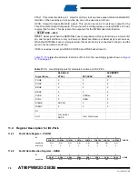
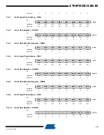
The Port D pins with alternate functions are shown in
.
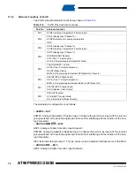
The alternate pin configuration is as follows:
• ACMP0 – Bit 7
ACMP0, Analog Comparator 0 Positive Input. Configure the port pin as input with the internal
pull-up switched off to avoid the digital port function from interfering with the function of the Ana-
log Comparator.
• ADC3/ACMPM/INT0 – Bit 6
ADC3, Analog to Digital Converter, input channel 3.
ACMPM, Analog Comparators Negative Input. Configure the port pin as input with the internal
pull-up switched off to avoid the digital port function from interfering with the function of the Ana-
log Comparator.
INT0, External Interrupt source 0. This pin can serve as an external interrupt source to the MCU.
• ADC2/ACMP2 – Bit 5
ADC2, Analog to Digital Converter, input channel 2.
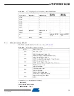
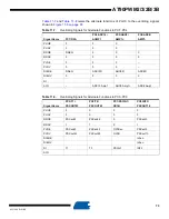
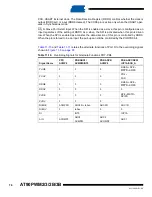
Table 11-9.
Port D Pins Alternate Functions
Port Pin
Alternate Function
PD7
ACMP0 (Analog Comparator 0 Positive Input )
PD6
ADC3 (Analog Input Channel 3 )
ACMPM reference for analog comparators
INT0
PD5
ADC2 (Analog Input Channel 2)
ACMP2 (Analog Comparator 2 Positive Input )
PD4
ADC1 (Analog Input Channel 1)
RXD (Dali/UART Rx data)
ICP1 (Timer 1 input capture)
SCK_A (Programming & alternate SPI Clock)
PD3
TXD (Dali/UART Tx data)
OC0A (Timer 0 Output Compare A)
SS (SPI Slave Select)
MOSI_A (Programming & alternate SPI Master Out Slave In)
PD2
PSCIN2 (PSC 2 Digital Input)
OC1A (Timer 1 Output Compare A)
MISO_A (Programming & alternate Master In SPI Slave Out)
PD1
PSCIN0 (PSC 0 Digital Input )
CLKO (System Clock Output)
PD0
PSCOUT00 output
XCK (UART Transfer Clock)
SS_A (Alternate SPI Slave Select)
Содержание AT90PWM2
Страница 344: ...346 4317I AVR 01 08 AT90PWM2 3 2B 3B 31 1 SO24...
Страница 345: ...347 4317I AVR 01 08 AT90PWM2 3 2B 3B 31 2 SO32...
Страница 346: ...348 4317I AVR 01 08 AT90PWM2 3 2B 3B 31 3 QFN32...
Страница 347: ...349 4317I AVR 01 08 AT90PWM2 3 2B 3B...


