Programmer’s Model
3-2
Copyright © 2002, 2003 ARM Limited. All rights reserved.
ARM DDI 0275D
3.1
About the programmer’s model
This section provides general information relevant to the ETB11 programmer’s model:
•
•
3.1.1
Register fields
You must not access reserved or unused address locations because this can result in
unpredictable behavior.
All reserved or unused bits of registers must be written as zero, and ignored on read
unless otherwise stated within the relevant text.
All registers bits are reset to a logic 0 by a reset unless otherwise stated in the relevant
text.
All registers support read and write accesses unless otherwise stated in the relevant text.
A write updates, and a read returns, the contents of the register.
3.1.2
Register map
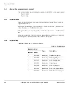
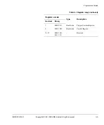
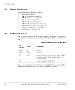
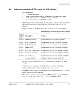
The ETB11 register map is shown in Table 3-1.
Table 3-1 Register map
Register number
Type
Description
Decimal
Binary
0
b000 0000
Read-only
Identification Register
1
b000 0001
Read-only
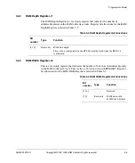
RAM Depth Register
2
b000 0010
Read-only
RAM Width Register
3
b000 0011
Read-only
Status Register
4
b000 0100
Read-only
RAM Data Register
5
b000 0101
Read/write
RAM Read Pointer Register
6
b000 0110
Read/write
RAM Write Pointer Register
Содержание ETB11
Страница 6: ...List of Tables vi Copyright 2002 2003 ARM Limited All rights reserved ARM DDI 0275D ...
Страница 8: ...List of Figures viii Copyright 2002 2003 ARM Limited All rights reserved ARM DDI 0275D ...
Страница 46: ...Functional Description 2 26 Copyright 2002 2003 ARM Limited All rights reserved ARM DDI 0275D ...
Страница 70: ...Signal Descriptions A 6 Copyright 2002 2003 ARM Limited All rights reserved ARM DDI 0275D ...
Страница 78: ...Glossary Glossary 4 Copyright 2002 2003 ARM Limited All rights reserved ARM DDI 0275D ...

