1
2
3
4
5
6
7
8
A
B
C
D
8
7
6
5
4
3
2
1
D
C
B
A
ISSUE
DRAWING NO.
23425
DRAWING TITLE
Drawn by:
DATE
Filename
ECO No.
DESCRIPTION OF CHANGE
J:\Change Control\ECO AGENDA\02 E000 L878 cap voltage correction\L878 3.3A.ddb - Documents\L878C6 3.3A.sch
A & R Cambridge Ltd.
Pembroke Avenue
Denny Industrial Centre
Waterbeach
Cambridge CB5 9PB
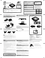
DVD AV PCB - Video (1)
Circuit Diagram
L878C6
PG
7-Jan-2002
INITIALS
Date Printed
6
7
Sheet
of
Notes:
5
6
7
Z22B
EL5244 SM
VS
8
GND
4
Z22C
EL5244 SM
VS
8
GND
4
Z23C
EL5244 SM
+
C92
470U EL 25V
Filters
Buffers
VID_GND
+5V_VID
VID_GND
5
6
7
Z23B
EL5244 SM
+
C93
470U EL 25V
VID_GND
3
2
1
Z23A
EL5244 SM
+
C94
470U EL 25V
VID_GND
3
2
1
Z22A
EL5244 SM
VIDEO (1)
+
C95
470U EL 25V
C98
100N 0805
C99
100N 0805
C100
100N 0805
VID_GND
5
6
7
Z24B
EL5244 SM
VS
8
GND
4
Z24C
EL5244 SM
+
C96
470U EL 25V
R108
75R 0805
R107
75R 0805
R106
75R 0805
R103
75R 0805
R109
75R 0805
VID_GND
R105
75R 0805
R104
75R 0805
R31
1K 0805
3
2
1
Z24A
EL5244 SM
R32
1K 0805
+
C97
470U EL 25V
R29
1K 0805
R30
1K 0805
R27
1K 0805
R28
1K 0805
R21
1K 0805
VID_GND
R22
1K 0805
R25
1K 0805
R26
1K 0805
R23
1K 0805
L3
2U2H SM
R24
1K 0805
VID_GND
VIDEO CONNECTOR
L4
2U2H SM
VID_GND
VID_GND
From DSP board
Q 41 QPAD
L5
2U2H SM
Q 40 QPAD
16/9: Indicate 16:9 ratio
ENABLE_AV: enable SCART AV
VID_GND
16/9
L6
2U2H SM
ENABLE_AV
VID_GND
L7
2U2H SM
V/ROUT
U/BOUT
Y/GOUT
VID_GND
SCART CVBS
CVBS_OUT
SVID COUT
SVID_YOUT
L8
2U2H SM
Q_39
QPAD
Q_38 QPAD
VID_GND
Q_37 QPAD
Q_36QPAD
Q_35QPAD
Q_34
QPAD
Q_33QPAD
VID_GND
V/RIN
1
2
3
4
5
6
7
8
9
10
11
12
13
14
15
16
17
18
19
20
21
22
SK2
FFC22V SM
U/BIN
Y/GIN
CVBS_IN
SVID_CIN
SVID_YIN
+
C28
100U EL SM
C31
100N 0805
C38
100N 0805
C144
100N 0805
C143
100N 0805
C145
100N 0805
C146 100N 0805
R1
75R 0805
R2
75R 0805
R3
75R 0805
R4
75R 0805
R18
75R 0805
R54
75R 0805
C119
22P NPO 0805
C120
22P NPO 0805
C121
22P NPO 0805
C122
22P NPO 0805
C123
22P NPO 0805
C124
22P NPO 0805
C113
270P NPO 0805
C114
270P NPO 0805
C115
270P NPO 0805
C116
270P NPO 0805
C117
270P NPO 0805
C118
270P NPO 0805
C107
330P NPO 0805
C108
330P NPO 0805
C109
330P NPO 0805
C110
330P NPO 0805
C111
330P NPO 0805
C112
330P NPO 0805
R113
0R0 0805
00_1136
PG
24/11/00 Issue 3 PCB with 8740 DACs
3.0
01_1000
PG
02/01/01 Change R9,R10 from 100R to 22R
3.1
01_1047
PG
15-03-01 Diodes changed from 3B22D to 3BS1D
3.2
PG
13/11/01 C155 changed to 100R
3.3
02_E000
PG
07/01/02 Admin change - cap voltages corrected on BOM
3.3A
Содержание DiVA DV88
Страница 1: ...DV88 DiVA DV88 DVD Player Progressive Scan Service Manual ARCAM Issue 2 0 ...
Страница 19: ...Diagram 2 points to solder to on DSP board ...
Страница 41: ...CAM Products 2000 TM L875pb 4 GTO ...
Страница 42: ......
Страница 43: ......
Страница 44: ......
Страница 45: ...CAM Products 2000 TM L889PB_2 GTO ...