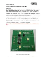
Figure 2: Picture of ADI USB-to-I2C Dongle (ADUSB2)
Setup Instructions:
Section 1 – Power Supply:
The SSM2529 evaluation board requires several different power supplies. The main power supplies required for
operation are PVDD (PVDD jack) and DVDD (DVDD jack). In addition to the main power supplies, there are several
other auxiliary power sections. The most basic setup for the SSM2529 evaluation board is to generate all onboard
power directly from PVDD utilizing jumper placements, eliminating the need for multiple power supplies. The correct
jumper settings for this mode are shown in Figure 3.
LDO_POWER: The SSM2529 board integrates two voltage regulators, U4 (3.3V) and U5 (1.8V). Note that the 3.3V
regulator powers most of the onboard digital audio interface circuitry. Inserting a jumper across J6 allows for PVDD to
power and activate these regulators. For current measurements on the PVDD pin of SSM2529, the device must be
isolated from this circuitry. In order to do so, remove the J6 jumper and connect an external power supply to J9 to
activate U4 and U5 voltage regulators.
ONBOARD_IOVDD: ONBOARD_IOVDD is a generalized power supply that is selected from the output of one of the
voltage regulators. ONBOARD_IOVDD can be selected as 1.8V or 3.3V by inserting a jumper across the designated
pins of J11. From that point, ONBOARD_IOVDD can be selected to power several different features: It can power
DVDD (J8), it can set the logic level of the onboard digital audio circuitry (J5), and it can be used as the I2C pull-up
voltage (J17).
DA_LEVEL: This is the logic level for the onboard digital audio signals. It can either be generated by
ONBOARD_IOVDD, as described above, or can be externally powered using J7. The logic level for these signals is
established on U7 – U10.
I2CVDD: This is the pull-up voltage for the I2C pins of SSM2529. This voltage can be set to either
ONBOARD_IOVDD or and external I2C pull-up by inserting a jumper across the designated pins of J17.


