background image

EVAL-AD7606C18FMCZ

 Evaluation Board User Guide 

UG-1870 


Rev. 0 | Page 11 of 15 

25052-

013


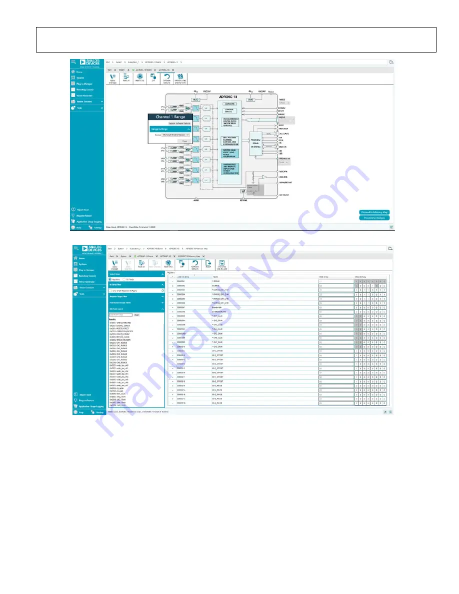
Figure 13. Configurable Pop-Up Window 

25052-

014


Figure 14. 

AD7606C-18 Memory Map

 View Window 

DESCRIPTION OF MEMORY MAP VIEW WINDOW 

Click 

Proceed to Memory Map

 in the 

AD7606C-18

 chip view 

window (see Figure 12) to open the 

AD7606C-18 Memory 

Map

 view window shown in Figure 14. Th

AD7606C-18 

Memory Map

 view window shows all registers of the 

AD7606C-18

. 

The registers of the AD7606C-18 are populated with default 
values when powered up. To implement the values changed in 
all of the registers, click 

Apply Changes

 to write to the registers. 

In some cases, the values of every register have been changed, 
but the user wants to implement changes on a selected register 

only. Click 

Apply Selected

 to write the new value on the 

selected register to the AD7606C-18. 
Click 

Read All

 to read the values of all the registers from the 

chip. 
Click 

Read Selected

 to read the selected register from the chip. 

Click 

Reset Chip

 to prompt the software to reset the AD7606C-18. 

Click 

Diff

 to check for differences in register values between 

the software and the chip. 
To revert all the register values back to their defaults, click 

Software Defaults

, and then click 

Apply Changes

 to write to 

the AD7606C-18. 


Содержание EVAL-AD7606C18FMCZ

Страница 1: ...NE RESOURCES ACE software AD7606C 18 ACE plugin provided in the ACE software AD7606x Family Software Model EVALUATION BOARD DESCRIPTION The EVAL AD7606C18FMCZ is a fully featured evaluation board that allows users to evaluate the features of the AD7606C 18 analog to digital converter ADC The EVAL AD7606C18FMCZ is controlled by the EVAL SDP CH1Z SDP H1 system demonstration platform SDP The SDP H1 c...

Страница 2: ...ation Board Hardware 4 Device Description 4 Hardware Link Options 4 Connectors and Sockets 4 Power Supplies 4 Channel Input 4 Evaluation Board Software 6 Software Installation 6 Evaluation Board Setup Procedures 8 ACE Software Operation 9 Launching the Software 9 Description of Chip View Window 9 Description of Memory Map View Window 11 Description of Analysis Window 12 Waveform Tab 12 Histogram T...

Страница 3: ...e Installation section 2 Ensure that the link options are configured as detailed in Table 2 3 Connect the SDP H1 to the EVAL AD7606C18FMCZ By default the power for the EVAL AD7606C18FMCZ is supplied by the SDP H1 See the Power Supplies section for the available power options 4 Connect the SDP H1 to the 12 V supply included in the SDP H1 kit and to the PC via the USB cable If prompted by the operat...

Страница 4: ...y FPGA mezzanine card FMC connector which connects the EVAL AD7606C18FMCZ to the SDP H1 POWER SUPPLIES Before applying power and signals to the EVAL AD7606C18FMCZ ensure that all link positions are set according to the required operating mode See Table 2 for the complete list of link options The supply required for the EVAL AD7606C18FMCZ comes from the SDP H1 Alternatively the EVAL AD7606C18FMCZ c...

Страница 5: ...g the on board U1 devices and must not be inserted if using the J9 SMB connector JP7 B JP7 selects the V1 line to be connected to ground single ended operation or to the SMB connector differential operation Position A connects the V1 line to ground for single ended operation Position B connects the V1 line to the J5 SMB connector and disconnects the V1 line from ground JP8 JP10 A Position A bypass...

Страница 6: ...E software take the following steps 1 Download the ACE software to a Windows based PC 2 Double click the ACEInstall exe file to begin the installation By default the software is saved to the following location C Program Files x86 Analog Devices ACE 3 A dialog box opens asking for permission to allow the program to make changes to the PC Click Yes to begin the installation process 4 In the ACE Setu...

Страница 7: ...Components 8 The Windows Security window opens see Figure 6 Click Install Figure 7 shows the installation in progress No action is required 25052 006 Figure 6 Windows Security Window 25052 007 Figure 7 Installation in Progress 9 When the installation is complete click Next see Figure 8 and then click Finish to complete the installation process 25052 008 Figure 8 Installation Complete ...

Страница 8: ...Verifying the Board Connection After connecting the power and the USB cable from the SDP H1 to the PC take the following steps to verify the SDP H1 connection 1 After connecting the SDP H1 to the PC allow the Found New Hardware Wizard to run Choose to automatically search for the drivers for the SDP H1 if prompted by the operating system 2 Navigate to the Device Manager window on the PC see Figure...

Страница 9: ...n in Figure 12 5 Click Software Defaults and then click Apply Changes to apply the default settings to the AD7606C 18 DESCRIPTION OF CHIP VIEW WINDOW After completing the steps in the Software Installation section set up the system for data capture Block icons that are dark blue are programmable blocks Clicking a dark blue block icon opens a configurable pop up window that allows customization for...

Страница 10: ...UG 1870 EVAL AD7606C18FMCZ Evaluation Board User Guide Rev 0 Page 10 of 15 25052 011 Figure 11 AD7606C 18 Board View 25052 012 Figure 12 AD7606C 18 Chip View Window ...

Страница 11: ... the values changed in all of the registers click Apply Changes to write to the registers In some cases the values of every register have been changed but the user wants to implement changes on a selected register only Click Apply Selected to write the new value on the selected register to the AD7606C 18 Click Read All to read the values of all the registers from the chip Click Read Selected to re...

Страница 12: ...user to select the data interface as either Parallel or Serial see Figure 16 If Serial is selected the number of data lines can be selected through the DOUT Configuration pulldown menu The Oversampling Ratio Software pulldown menu in the Device Configuration section can be set between 2 and 64 in hardware mode or 256 in software mode and provides improved signal to noise ratio SNR performance see ...

Страница 13: ...ithin the sampled data see Figure 17 The Histogram graph is useful for dc analysis and indicates the noise performance of the AD7606C 18 FFT TAB The FFT tab displays the fast Fourier transform FFT information for the last batch of samples gathered see Figure 18 ANALYSIS Pane The General Settings section allows the user to set up the preferred configuration of the FFT analysis including how many to...

Страница 14: ...UG 1870 EVAL AD7606C18FMCZ Evaluation Board User Guide Rev 0 Page 14 of 15 25052 016 Figure 16 Waveform Tab 25052 017 Figure 17 Histogram Tab ...

Страница 15: ... any other party for any reason Upon discontinuation of use of the Evaluation Board or termination of this Agreement Customer agrees to promptly return the Evaluation Board to ADI ADDITIONAL RESTRICTIONS Customer may not disassemble decompile or reverse engineer chips on the Evaluation Board Customer shall inform ADI of any occurred damages or any modifications or alterations it makes to the Evalu...

Отзывы: