


UG-1882
Rev. 0 | Page 9 of 28
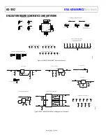
LINK CONFIGURATION OPTIONS
Take care before applying power and signals to the EVAL-
AD4696FMCZ to ensure all solder link positions are set as
required by the operating mode. Table 8 lists the solder link
functions on the EVAL-AD4696FMCZ hardware, and indicates
the default positions in which the links are set as manufactured.
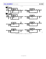
Table 8. Links, Factory Default Settings
Link
Default Function
Comment
JP0,
JP1
A
Connects the inverting inputs of the IN0 and IN1 channel ADC
drivers (A0) to SMA inputs (J1 or J3, and J2 or J4) or board ground.
Default state is SMA input.
Change to B to tie the inverting input to ground
(populate R13 = R14 = 0 Ω as well).
JP2
A
Used to enable or disable the on-board VREF/2 divider (A8,
The VREF/2 divider must be enabled when configuring an
channel in pseudobipolar mode and paired with COM. Default state
is enabled.
Change to B to disable the VREF/2 divider.
JP3
A
Used to enable or disable the dc bias generator for Channel 0 to
Channel 7 (U7,
). Default state is enabled.
Change to B to disable the dc bias generator for IN0 to IN7.
JP4
A
Used to enable or disable the on-board reference buffer (A10,
ADA4807-1). Default state is enabled.
Change to B to disable the on-board reference buffer.
JP5
A
Used to enable or disable the dc bias generator for Channel 8 to
Channel 15 (U9, ADA4841-1). Default state is enabled.
Change to B to disable the dc bias generator for IN8 to
IN15.
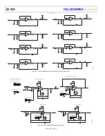
JP6
B
Connects the COM pin of the ADC to ground or the output of the
VREF/2 buffer (A8). See the Hardware Configurations for Supporting
AD4696 Polarity Modes section for instructions on selecting the
appropriate position of JP6.
Change to A to connect the COM pin to VREF/2 V.
JP7
A
Connects LDO_IN to AVDD or AGND. By default, the internal LDO is
enabled because LDO_IN is connected to AVDD and VDD is floating.
To disable the internal LDO regulator, connect LDO_IN to AGND.
Change to B to connect LDO_IN to AGND
JP8
A
Connects VIO to 1.8 V on board (U6,
) or VADJ. By default, VIO
is connected to 1.8 V on board.
Change to B to connect VIO to VADJ.
JP9
A
Used to enable or disable
(U2) LDO regulator on board. By
default, this LDO is enabled. If powering the 7.5 V test point using an
external source, this LDO can be disabled.
Change to B to disable the LDO.
JP11
B
Used to select between on-board reference (U3,
) and
external reference (P5). By default, the on-board reference is connected.
Change to A to use external reference.
JP12
A
Selects between the on-board 7.5 V and 5 V voltage rails for +VS
Bank A. Default state is 7.5 V.
+VS Bank A connects to the positive supply pins of A0 to
A3. Change JP12 to Position B to select 5 V. See the Setting
Amplifier Supply Voltages section for more information.
JP13
A
Selects between the on-board −2.5 V voltage rail and ground for
−VS Bank A. Default state is −2.5 V.
−VS Bank A connects to the negative supply pins of A0
to A3. Change JP13 to Position B to select ground. See the
Setting Amplifier Supply Voltages section for more
information.
JP14
A
Selects between the on-board 7.5 V and 5 V voltage rails for +VS
Bank B. Default state is 7.5 V.
+VS Bank B connects to the positive supply pins of A4 to
A7. Change JP14 to Position B to select 5 V. See the Setting
Amplifier Supply Voltages section for more information.
JP15
A
Selects between the on-board −2.5 V voltage rail and ground for
−VS Bank B. Default state is −2.5 V.
−VS Bank B connects to the negative supply pins of A4
to A7. Change JP15 to Position B to select ground. See the
Setting Amplifier Supply Voltages section for more
information.
JP16
A
Selects between the on-board 7.5 V and 5 V voltage rails for +VS
Bank C. Default state is 7.5 V.
+VS Bank C connects to the positive supply pins of A8,
A10, U7, and U9. Change JP16 to Position B to select 5 V.
See the Setting Amplifier Supply Voltages section for
more information.
JP17
A
Selects between the on-board −2.5 V voltage rail and ground for
−VS Bank C. Default state is −2.5 V.
−VS Bank C connects to the negative supply pins of A8,
A10, U7, and U9. Change JP17 to Position B to select
ground. See the Setting Amplifier Supply Voltages
section for more information.
JP31
B
Connects CNV and CS_N signals for 4-wire SPI operation (see the 4-
Wire SPI Operation section). By default, the CNV and CS_N signals
are not connected to each other.
Change to Position A to connect the CS_N and CNV
signals.


