Analog Devices EVAL-AD4696FMCZ Скачать руководство пользователя страница 8

UG-1882 

EVAL-AD4696FMCZ

 User Guide 


Rev. 0 | Page 8 of 28 

regulator is enabled and supplies VDD with 1.8 V automatically on 
power-up.  

To configure the hardware to utilize the on-board regulator instead 
of th

AD4696

 internal LDO regulator, the R27 resistor can be 

populated with 0 Ω, connecting the (1.8 V) output of the 

LT1761


to VDD. The internal LDO regulator of the AD4696 can then be 
disabled in the AD4696 

ACE

 plugin by setting the LDO_EN bit 

to 0. It is worth noting that because the internal LDO regulator of 
the AD4696 is enabled by default, when the EVAL-AD4696FMCZ 
is powered up in this configuration, the VDD pin of the AD4696 
is simultaneously driven by its internal LDO regulator and the 
on-board 1.8 V supply. For this reason, the internal LDO regulator 
of the AD4696 is designed to withstand being driven by an external 
1.8 V supply while enabled, but it is recommended to ground the 
LDO_IN input by changing the position of JP7 to ensure the 
internal LDO regulator output is not driven at power-up. 

See the AD4696 data sheet for more information on the 
operation of the internal LDO. 

Powering EVAL-AD4696FMCZ Externally 

All of the active devices can be disconnected from the on-board 
power circuitry on the EVAL-AD4696FMCZ to enable external 
power options (for example, a bench top supply). The voltage 
rails (for example, +7.5 V, +5 V, +1.8 V, and −2.5 V) can be powered 
externally by removing the 0 Ω resistors at the outputs of the power 
management ICs that generate them (see Table 7 for the list). 
The supply pins of the on-board reference, the AD4696, and the 
amplifier supply banks, can also be disconnected from the 
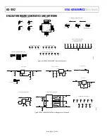
on-board supplies in the same way. See the schematic in Figure 25 
to locate the relevant components for powering each voltage rail 
and component supplies. 

Table 7. Resistors to Disconnect Voltage Rails from 
On-Board Supplies 

Supply Rail (V) 

Resistor 

7.5 R123 

5 R129 

1.8 R135 

−2.5 R130 

Powering the EVAL-AD4696FMCZ with Other FMC- or 
PMOD-Compatible Controller Boards 

The 

EVAL-SDP-CH1Z

 provides the 3.3 V (VCC_HOST) and 

12 V supply (VPWR_12V) to the EVAL-AD4696FMCZ through 
the FMC connector (P1). The EVAL-AD4696FMCZ can also be 
powered by 3.3 V supplies from other FMC-compatible or 
PMOD-compatible controller boards (via P1 and P30, respectively) 
and by 12 V supplies through the VPWR test point (remove 
R31) or via P1. Before connecting other controller boards to the 
EVAL-AD4696FMCZ, ensure that their supplies are the correct 
voltages and have adequate current sourcing capabilities.  

The current required by the EVAL-AD4696FMCZ hardware 
depends on the configuration of on-board circuitry (for example, 
populated ADC driver amplifiers and number of on-board vs. 
external power supplies).  

DIGITAL INTERFACE 

The EVAL-AD4696FMCZ provides access to the AD4696 digital 
interface pins via a 160-pin field programmable gate array (FPGA) 
mezzanine card (FMC) connector (P1) and alternatively via a 
12-pin extended SPI PMOD-compatible connector (P30). 

The AD4696 ACE plugin communicates to the EVAL-
AD4696FMCZ hardware via the SDP-H1 board through a 160-pin 
FMC connector (P1). The software and hardware are designed 
to quickly and easily connect and enable evaluation of the AD4696. 

Alternatively, the user can use a PMOD-compatible device to 
communicate with the AD4696 through P30. If the user chooses 
to use a PMOD-compatible device, ensure that the pin 
assignments match those on the P30 connector. 

Setting the AD4696 Logic Voltage (VIO) 

The output logic levels of the AD4696 are set by the voltage 
applied to its VIO pin, which can range from 1.2 V to 1.8 V (see 
the AD4696 data sheet for detailed VIO specifications). The 
EVAL-AD4696FMCZ provides several means to drive VIO. 

By default, VIO is driven by the on-board, 1.8 V LDO regulator 
(U6, LT1761). Changing the position of Solder Link JP8 (see 
Figure 24) allows the VADJ pin on the FMC connector (Pin G39) 
to drive VIO instead. Both options are compatible with the SDP-H1 
that is used in conjunction with the AD4696 evaluation software. 
Using VADJ also allows the EVAL-AD4696FMCZ to interface 
with third party FMC-compatible controller boards, provided 
VADJ can be set within the acceptable range of the VIO pin (see 
the Using Third Party Controller Boards section). 

4-Wire SPI Operation 

The AD4696 can be operated using only four SPI signals, if 
desired, by driving CNV and CS with the same signal. The 
EVAL-AD4696FMCZ enables this mode by changing the default 
position of JP31. Note that the AD4696 evaluation software 
does not support this option, and it is intended for use only with 
third party controller boards with a 4-wire SPI peripheral (see the 
Using Third Party Controller Boards section). 

Using Third Party Controller Boards 

The EVAL-AD4696FMCZ hardware largely follows VMEbus 
International Trade Association (VITA) standards with the 
FMC pin-to-signal assignments and with the board width on 
the side with the FMC connector (P1). The pinout on the PMOD 
connector (P30) follows the PMOD extended SPI standard. By 
following these standards as much as possible, the EVAL-
AD4696FMCZ allows mating of the AD4696 with other common 
controller boards. If using an FMC-compatible controller board 
other than the SDP-H1, ensure that its logic levels and VADJ pin 
(Pin G39) can be set to between 1.2 V and 1.8 V. It is also 
recommended to use a cable to interface PMOD-compatible 
controller boards to the PMOD header on the evaluation board. 

Note that when using PMOD-compatible boards, it is necessary 
to supply the 12 V VPWR supply externally through the VPWR 
test point. 

Содержание EVAL-AD4696FMCZ

Страница 1: ...S multiplexed successive approximation register SAR analog to digital converter ADC that enables high performance data acquisition of multiple signals in a small form factor The AD4696 employs easy drive features and on chip channel sequencing that simplify hardware and software designs and allow it to fit into a variety of space constrained precision multichannel applications The EVAL AD4696FMCZ ...

Страница 2: ...eference 7 Power Supplies 7 Digital Interface 8 Link Configuration Options 9 Getting Started 10 Software Installation 10 Evaluation Hardware Setup Procedure 13 Evaluation Software Operation 14 Launching the AD4696 ACE Plugin 14 Description of Chip View 14 Sequencer Configuration Views 14 Channel Configuration View 17 Analysis View 18 Waveform Tab 20 Histogram Tab 20 FFT Tab 20 Memory Map View 20 E...

Страница 3: ...EVAL AD4696FMCZ User Guide UG 1882 Rev 0 Page 3 of 28 EVAL AD4696FMCZ PHOTOGRAPH 25058 001 Figure 1 ...

Страница 4: ...evaluated with the AD4696 on the EVAL AD4696FMCZ Channel IN0 and Channel IN1 have been configured to demonstrate ac performance of the AD4696 whereas Channel IN2 through Channel IN15 have been configured to demonstrate simple noise measurements and signal settling measurements with dc voltages generated on board The amplifiers driving Channel IN0 and Channel IN1 can be configured to perform common...

Страница 5: ...e performance and settling accuracy performance when sequencing the multiplexer between channels or channel configurations There are two dc signals labeled CHDR1 and CHDR2 in Figure 26 Figure 27 and Figure 28 CHDR1 and CHDR2 are generated by two ADA4841 1 devices configured as unity gain buffers U7 and U9 in Figure 28 The inputs of U7 and U9 are connected to the output of the voltage reference U3 ...

Страница 6: ...6 selects whether the COM pin is connected directly to the EVAL AD4696FMCZ ground for example 0 V or the VREF 2 V output of A8 Ensure that JP6 is configured appropriately for the channel configuration settings selected via the AD4696 evaluation software By default the COM pin is connected to AGND through JP6 When pairing even and odd numbered inputs modify the resistor divider components on the in...

Страница 7: ...are connected to one of a set of three positive and three negative supply banks and the voltage of the banks can be selected via solder links shown in Figure 29 and Table 6 These banks provide users a way of configuring the on board amplifiers with different power supply voltages For example tying the amplifier negative supplies to ground the user can evaluate the performance of the AD4696 in unip...

Страница 8: ... number of on board vs external power supplies DIGITAL INTERFACE The EVAL AD4696FMCZ provides access to the AD4696 digital interface pins via a 160 pin field programmable gate array FPGA mezzanine card FMC connector P1 and alternatively via a 12 pin extended SPI PMOD compatible connector P30 The AD4696 ACE plugin communicates to the EVAL AD4696FMCZ hardware via the SDP H1 board through a 160 pin F...

Страница 9: ...ct VIO to VADJ JP9 A Used to enable or disable ADP7142 U2 LDO regulator on board By default this LDO is enabled If powering the 7 5 V test point using an external source this LDO can be disabled Change to B to disable the LDO JP11 B Used to select between on board reference U3 ADR4550 and external reference P5 By default the on board reference is connected Change to A to use external reference JP1...

Страница 10: ...n software take the following steps 1 Download the ACE evaluation software to a Windows based PC 2 Double click the ACEInstall exe file to begin the installation By default the software is saved to C Program Files x86 Analog Devices ACE 3 A dialog box appears asking for permission to allow the program to make changes to the PC Click Yes to begin the installation process 4 Click Next to continue th...

Страница 11: ...lect All Programs Analog Devices ACE ACE exe which brings up the window shown in Figure 13 2 To install the AD4696 ACE plugin click Plug in Manager on the left of the ACE main window as shown in Figure 10 3 Select the Available Packages drop down menu on the left and search for AD4696 using the search text box on the right as shown in Figure 11 the AD4696 plugin is not shown as an option in Figure...

Страница 12: ...UG 1882 EVAL AD4696FMCZ User Guide Rev 0 Page 12 of 28 25058 011 Figure 10 Selecting Plug in Manager 25058 012 Figure 11 Installing AD4696 ACE Plugin 25058 013 Figure 12 Updating AD4696 ACE Plugin ...

Страница 13: ... AD4696 ACE plugin Verifying Hardware Connection To verify the EVAL AD4696FMCZ is properly connected to the PC take the following steps 1 Allow the Found New Hardware Wizard to finish running after the SDP H1 is connected to the PC via the USB cable Choose the Automatically Search for the Appropriate Drivers option for the SDP drivers if prompted 2 Verify the hardware to PC connection by navigatin...

Страница 14: ...iption of the Standard Sequencer View section and the Description of the Advanced Sequencer View section The Configure Channels button opens the Channel Configuration view see the Channel Configuration View section The Proceed to Analysis button opens the AD4696 Analysis view see the Analysis View section The Proceed to Memory Map button opens the AD4696 Memory Map view see the Memory Map View sec...

Страница 15: ...EVAL AD4696FMCZ User Guide UG 1882 Rev 0 Page 15 of 28 25058 014 Figure 13 ACE Software Start Window 25058 015 Figure 14 Evaluation Board View 25058 016 25058 016 Figure 15 Chip View ...

Страница 16: ...view appears as shown in Figure 17 Use the Number of Slots text box to enter the number of desired slots in the sequence Select the desired channel for each slot using the slot assignment dropdown menus Click Apply Changes to configure the connected device accordingly The number of slot assignment dropdown boxes that are enabled or disabled is determined by the value in the Number of Slots text bo...

Страница 17: ... Figure 18 and Figure 19 The controls that are visible in the All Channel Controls tab vs the controls visible in the Controls for Channel tab depends on the active sequencer mode standard sequencer vs advanced sequencer to reflect how these settings are applied differently based on the channel sequencer mode See the AD4696 data sheet for a detailed description on how the channel sequencing mode a...

Страница 18: ...r Threshold Value text box accepts 12 bit hexadecimal values between 0x000 and 0xFFF The value entered in this text box is written to the lower bit field in the corresponding LOWER_INn register The Hysteresis Value text box accepts 12 bit hexadecimal values between 0x000 and 0xFFF The value entered in this text box is written to the hysteresis bit field in the corresponding HYST_INn register When ...

Страница 19: ...on The Sequencer Mode dropdown box allows the user to select the desired sequencer mode Clicking the Go to Sequencer button opens either the standard sequencer view or the advanced sequencer view based on the value selected in the Sequencer Mode dropdown menu Reference Settings Use the Reference Voltage text box to enter the value of the reference voltage on the connected hardware The Reference Vo...

Страница 20: ...rm Graph The data waveform graph shows each successive sample of the ADC output The user can zoom and pan the waveform using the embedded waveform tools The channels to display can be selected in Display Channels Display Units and Axis Controls Click the display units dropdown list to select whether the data graph displays in units of Hex volts or codes decimal see Figure 20 HISTOGRAM TAB Click th...

Страница 21: ...f Click Diff to check for difference in register values between software and the connected AD4696 Clicking Diff performs a read of the full register map of the connected device and compares the bit field states to those reported in the memory map view Software Defaults Click Software Defaults to update the bit fields in the memory map view to their default states Clicking Software Defaults only up...

Страница 22: ... 28 25 4 24 20 14 13 AGND AGND AGND AGND AGND AGND AGND AGND B COM A B COM A AGND B COM A AGND PAD IN4 IN3 IN2 IN1 IN0 REF REFGND CS CNV SDI SCK SDO BSY_ALT_GP0 IOGND VIO RESET VDD LDO_IN AVDD AGND IN15 IN14 IN13 IN12 IN11 IN10 IN9 IN8 COM IN7 IN6 IN5 10UF 10UF 10UF 10UF 25058 027 CS Figure 24 EVAL AD4696FMCZ Top Level Schematic 3 3V 3 3V VOLTAGE INVERTER 5V 1 8V LDO 12V 7 5V LDO POWER SUPPLY TEST...

Страница 23: ...NI 10K 0 0 0 10K 0 C87 C32 C70 C86 C19 C18 R20 R108 R109 R110 R111 R106 R107 R16 R15 R24 R23 A3 R44 R43 R48 R52 A3 R47 R51 C43 C42 R7 R5 R19 A2 R42 R41 R46 R50 A2 R45 R49 C41 C40 A1 A1 A0 A0 R8 R12 R32 R36 R30 R40 C39 R6 R11 R35 R39 C38 R4 R10 R18 C35 R28 JP1 R3 C36 R14 C34 R22 R34 C33 R38 C31 R21 R13 JP0 C30 C29 R37 R33 R17 R26 C37 R1 R2 R9 CHDR1 CH0 IN0 CH0 CHDR1 IN6 CHDR1 CHDR1 CHDR1 CHDR1 IN1 ...

Страница 24: ... 27 EVAL AD4696FMCZ Driver Amplifier Schematic IN8 to IN15 DC BIAS CH0 CH7 ON BOARD REFERENCE BUFFER VREF 2 DIVIDER CIRCUIT DC BIAS CH8 CH15 DEFAULT POSITION B DEFAULT POSITION A DEFAULT POSITION A EXTERNAL REFERENCE TERMINAL BLOCK ON BOARD OR EXTERNAL REFERENCE REFERENCE SOURCE OPTIONS DEFAULT POSITION A DEFAULT POSITION A 0 2700PF DNI DNI 2700PF 2700PF 2700PF DNI 2700PF DNI DNI 0 10 0 ADA4841 1Y...

Страница 25: ... AGND AGND B COM A 25058 032 Figure 29 EVAL AD4696FMCZ Amplifier Power Supply Jumper Selection Schematic DEFAULT POSITION B CONNECT CS AND CNV FOR 4 WIRE OPERATION 12 PIN DIGITAL HEADER DIGITAL HOST CONNECTIONS FMC 160 PIN CONNECTOR EEPROM 3PINJUMPER_0603 0 1UF ASP 134604 01 ASP 134604 01 ASP 134604 01 M24C02 RMN6TP ASP 134604 01 TSW 106 08 G D JP31 P30 C151 U8 P1 P1 P1 P1 CNV_FMC CNV CS_N CS_N CN...

Страница 26: ...82 EVAL AD4696FMCZ User Guide Rev 0 Page 26 of 28 25058 034 Figure 31 EVAL AD4696FMCZ Silkscreen Top Assembly 25058 036 Figure 32 EVAL AD4696FMCZ Top Layer 25058 037 Figure 33 EVAL AD4696FMCZ Layer 2 Ground ...

Страница 27: ...EVAL AD4696FMCZ User Guide UG 1882 Rev 0 Page 27 of 28 25058 038 Figure 34 EVAL AD4696FMCZ Layer 3 Power 25058 039 Figure 35 EVAL AD4696FMCZ Bottom Layer ...

Страница 28: ...rty for any reason Upon discontinuation of use of the Evaluation Board or termination of this Agreement Customer agrees to promptly return the Evaluation Board to ADI ADDITIONAL RESTRICTIONS Customer may not disassemble decompile or reverse engineer chips on the Evaluation Board Customer shall inform ADI of any occurred damages or any modifications or alterations it makes to the Evaluation Board i...

Отзывы: