


AD5934
Rev. A | Page 14 of 40
FREQUENCY SWEEP COMMAND SEQUENCE
The following sequence must be followed to implement a
frequency sweep:
1.
Enter standby mode. Prior to issuing a start frequency sweep
command, the device must be placed in standby mode by
issuing an enter standby mode command to the control
register (Register Address 0x80 and Register Address 0x81).
In this mode, the VOUT and VIN pins are connected internally
to ground so there is no dc bias across the external impedance or
between the impedance and ground.
2.
Enter initialize mode. In general, high Q complex circuits
require a long time to reach steady state. To facilitate the
measurement of such impedances, this mode allows the user
full control of the settling time requirement before entering
start frequency sweep mode where the impedance
measurement takes place.
An initialize with start frequency command to the control
register enters initialize mode. In this mode, the impedance
is excited with the programmed start frequency but no
measurement takes place. The user times out the required
settling time before issuing a start frequency sweep command to
the control register to enter the start frequency sweep mode.
3.
Enter start frequency sweep mode. The user enters this mode
by issuing a start frequency sweep command to the control
register. In this mode, the ADC starts measuring after the
programmed number of settling time cycles elapses. The user
can program an integer number of output frequency cycles
(settling time cycles) to Register Address 0x8A and Register
Address 0x8B before beginning the measurement at each
frequency point (see Figure 30).
The DDS output signal is passed through a programmable
gain stage to generate the four ranges of peak-to-peak output
excitation signals listed in Table 5. The peak-to-peak output
excitation voltage is selected by setting Bit D10 and Bit D9 in
the control register (see the Control Register section) and is
made available at the VOUT pin.
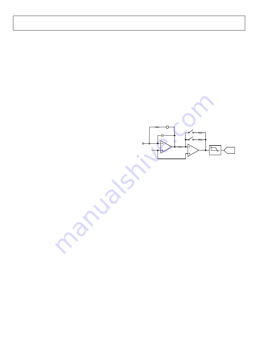
RECEIVE STAGE
The receive stage comprises a current-to-voltage amplifier,
followed by a programmable gain amplifier (PGA), antialiasing
filter, and ADC. The receive stage schematic is shown in Figure 17.
The unknown impedance is connected between the VOUT and
VIN pins. The first stage current-to-voltage amplifier configuration
means that a voltage present at the VIN pin is a virtual ground
with a dc value set at VDD/2. The signal current that is developed
across the unknown impedance flows into the VIN pin and
develops a voltage signal at the output of the current-to-voltage
converter. The gain of the current-to voltage amplifier is determined
by a user-selectable feedback resistor connected between Pin 4
(RFB) and Pin 5 (VIN). It is important for the user to choose a
feedback resistance value which, in conjunction with the selected
gain of the PGA stage, maintains the signal within the linear range
of the ADC (0 V to VDD).
05
32
5-
0
38
5 × R
R
R
R
C
VIN
VDD/2
RFB
ADC
LPF
Figure 17. Receive Stage
The PGA allows the user to gain the output of the current-to-
voltage amplifier by a factor of 5 or 1 depending upon the status
of Bit D8 in the control register (see the Register Map section
Register Address 0x80). The signal is then low-pass filtered and
presented to the input of the 12-bit, 250 kSPS ADC.
The digital data from the ADC is passed directly to the DSP core
of the AD5934 that performs a DFT on the sampled data.
DFT OPERATION
A DFT is calculated for each frequency point in the sweep. The
AD5934 DFT algorithm is represented by
(
)
))
sin(
)
)(cos(
(
)
(
1023
0
n
j
n
n
x
f
X
n
−
=
∑
=
where:
X
(
f
) is the power in the signal at the Frequency Point
f
.
x
(
n
) is the ADC output.
cos(
n
) and sin(
n
) are the sampled test vectors provided by the
DDS core at the Frequency
f
.
The multiplication is accumulated over 1024 samples for each
frequency point. The result is stored in two 16-bit registers
representing the real and imaginary components of the result. The
data is stored in twos complement format.
Содержание AD5934
Страница 35: ...AD5934 Rev A Page 35 of 40 SCHEMATICS 05325 144 Figure 40 EVAL AD5934EBZ USB Schematic ...
Страница 36: ...AD5934 Rev A Page 36 of 40 05325 145 Figure 41 EVAL AD5934EBZ Schematic ...
Страница 37: ...AD5934 Rev A Page 37 of 40 05325 146 Figure 42 Linear Regulator on EVAL AD5934EBZ ...
Страница 38: ...AD5934 Rev A Page 38 of 40 05325 147 Figure 43 Decoupling on the EVAL AD5934EBZ ...